Solid state imaging device, driving method of the solid state imaging device, and electronic equipment

a solid-state imaging and driving method technology, applied in the direction of radioation control devices, television system scanning details, television systems, etc., can solve the problems of marked deterioration in photographed image quality, improve image quality of imaged images, and reduce noise due to irregularities in the threshold value of pixel transistors among pixels.

Active Publication Date: 2009-10-08
SONY CORP
View PDF10 Cites 118 Cited by
  • Summary
  • Abstract
  • Description
  • Claims
  • Application Information

AI Technical Summary

Benefits of technology

[0032]The photo-generated charge generated by photoelectric conversion at the photoelectric converter is held in the photoelectric converter when the illuminance is low and the charge is at or below a predetermined charge. In the event that the illuminance is high and the charge exceeds the predetermined charge amount, the portion thereof which exceeds the predetermined charge amount is transferred to the charge holding region as a first signal charge. Accordingly, the photo-generated charge generated by photoelectric conversion is divided and accumulated as a first signal charge in the charge holding region and a second signal charge in the photoelectric converter. Now, while irregularities in the threshold value of the first transfer gate which is a pixel transistor does affect the charge being accumulated in the charge holding region, there is no effect on the final unit pixel input/output properties. For example, let us say that that the entire charge amount at a certain p

Problems solved by technology

Even if global exposure is realized, reduction in the dynamic range, which is an important

Method used


Image

  • Solid state imaging device, driving method of the solid state imaging device, and electronic equipment
  • Solid state imaging device, driving method of the solid state imaging device, and electronic equipment
  • Solid state imaging device, driving method of the solid state imaging device, and electronic equipment

Examples


application example

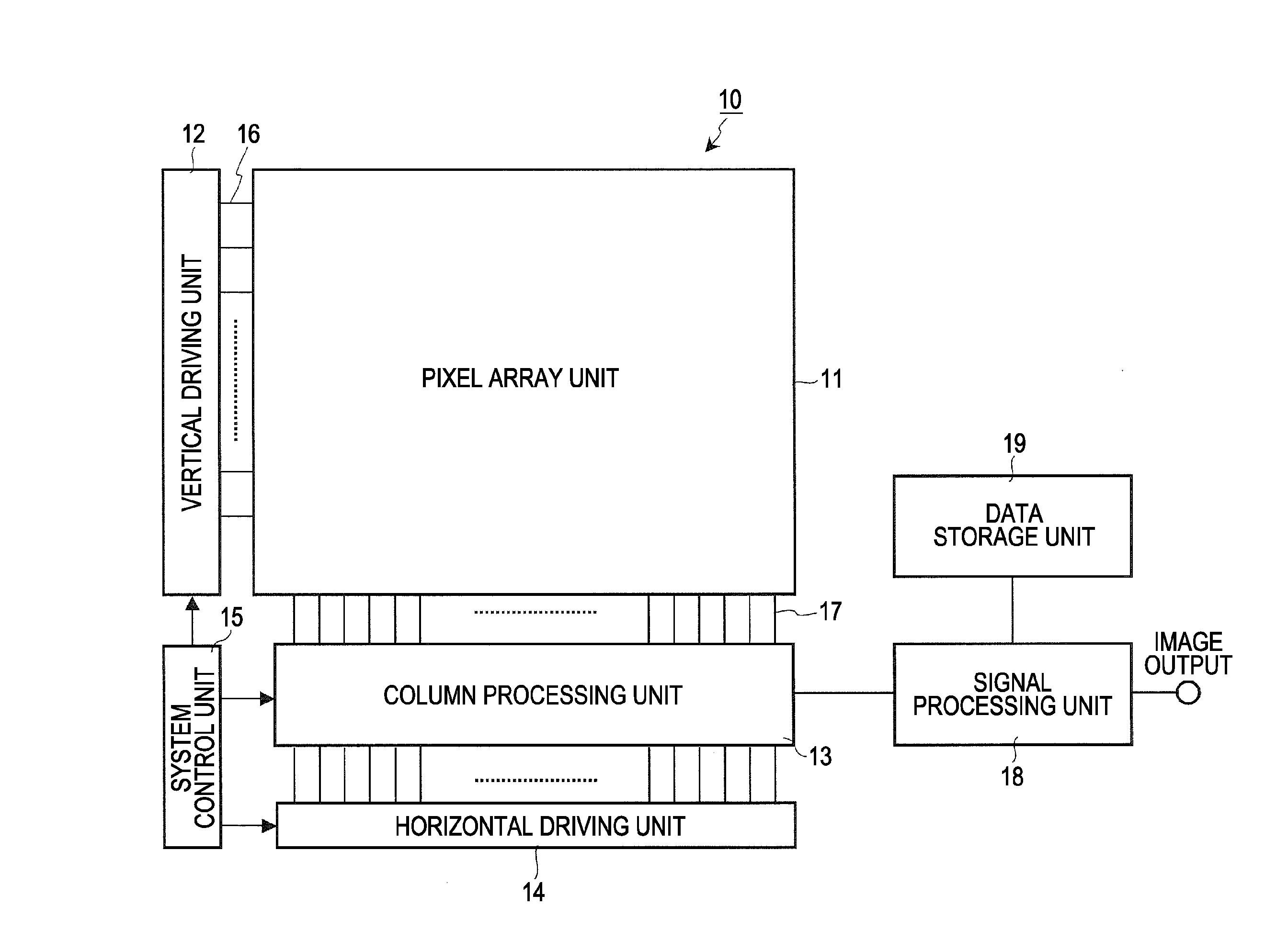
[0276]FIG. 37 is a block diagram illustrating an example of a configuration of electronic equipment according to an embodiment of the present invention, such as an imaging apparatus for example. As shown in FIG. 37, an imaging apparatus according to an embodiment of the present invention includes an optical system having a lens group 51 and the like, an imaging device 52, a DSP circuit 53 which is a camera signal processing circuit, frame memory 54, a display device 55, a recording device 56, an operating system 57, a power source system 58, and so forth, with the DSP circuit 53, frame memory 54, display device 55, recording device 56, operating system 57, and power supply system 58 being connected mutually by a bus line 59.

[0277]The lens group 51 inputs incident light (image light) from a subject and images this on the imaging face of the imaging device 52. The imaging device 52 converts the luminous quantity of the incident light aimed on the imaging face by the lens group 51 into...


PUM


Abstract

A solid state imaging device includes: multiple unit pixels including a photoelectric converter generating electrical charge in accordance with incident light quantity and accumulating the charge, a first transfer gate transferring the accumulated charge, a charge holding region holding the transferred charge, a second transfer gate transferring the held charge, and a floating diffusion region converting the transferred charge into voltage; an intermediate charge transfer unit transferring, to the charge holding region, a charge exceeding a predetermined charge amount as a first signal charge; and a pixel driving unit setting the first transfer gate to a non-conducting state, set the second transfer gate to a conducting state, transfer the first signal charge to the floating diffusion region, set the second transfer gate to a non-conducting state, set the first transfer gate to a conducting state, and transfer the accumulated charge to the charge holding region as a second signal charge.

Description

BACKGROUND OF THE INVENTION[0001]1. Field of the Invention[0002]The present invention relates to a solid state imaging device, a driving method of the solid state imaging device, and electronic equipment.[0003]2. Description of the Related Art[0004]An example of a solid-state imaging device is a CMOS image sensor which reads out photo-generated charges accumulated in the p-n junction capacitance of photodiodes, which are photoelectric conversion devices, by way of MOS transistors. With such a CMOS image sensor, actions for reading out photo-generated charges accumulated in photodiodes are executed for each pixel, each line, or the like. Accordingly, the exposure period for accumulating photo-generating charge does not match for all pixels, and distortion occurs in the image when the subject is moving, etc.[0005]FIG. 38 illustrates a structural example of a unit pixel (hereinafter may be referred to simply as “pixel”). As shown in FIG. 38, the unit pixel 100 is of a configuration inc...

Claims


Application Information

Patent Timeline
IPC IPC(8): H04N5/335H01L27/146H04N5/365
CPCH01L27/14609H01L27/14643H01L27/14654H01L27/148H04N3/1568H04N5/335H04N5/3651H04N3/155H04N25/583H04N25/65H04N25/671H04N25/771H01L27/146H04N25/00
Inventor OIKE, YUSUKE
Owner SONY CORP
Why Eureka
Try Eureka