Light-emitting element, display device, and electronic apparatus

a technology of light-emitting elements and display devices, applied in the direction of organic semiconductor devices, identification means, instruments, etc., can solve the problems of low durability of light-emitting elements, and achieve the effects of good balance, excellent reliability, and reduced driving voltage of light-emitting elements

Active Publication Date: 2009-10-22
INTELLECTUAL KEYSTONE TECH LLC
View PDF1 Cites 59 Cited by
  • Summary
  • Abstract
  • Description
  • Claims
  • Application Information

AI Technical Summary

Benefits of technology

[0006]An advantage of some aspects of the invention is that it provides a light-emitting element which includes three or more laminated light-emitting layers, which has excellent durability and luminous efficiency, and in which the light-emitting layers emit light with good balance, and a display device and electronic apparatus including the light-emitting element and having high reliability.
[0007]A light-emitting element according to a first aspect of the invention includes a cathode, an anode, a first light-emitting layer that is disposed between the cathode and the anode and that emits light of a first color, a second light-emitting layer that is disposed between the first light-emitting layer and the cathode and that emits light of a second color different from the first color, a third light-emitting layer that is disposed between the second light-emitting layer and the cathode and that emits light of a third color different from the first color and the second color, a first interlayer that is disposed between the first light-emitting layer and the second light-emitting layer so as to be in contact with the first and second light-emitting layers and that has a function of preventing energy transfer of an exciton between the first light-emitting layer and the second light-emitting layer, and a second interlayer that is disposed between the second light-emitting layer and the third light-emitting layer so as to be in contact with the second and third light-emitting layers and that has a function of preventing energy transfer of an exciton between the second light-emitting layer and the third light-emitting layer, wherein the first interlayer has a hole-transporting property higher than that of the second interlayer, and the second interlayer has an electron-transporting property higher than that of the first interlayer. Accordingly, in a structure including laminated three or more light-emitting layers, light can be emitted from each of the light-emitting layers with good balance while realizing excellent durability and luminous efficiency.
[0008]The energy level of the highest occupied molecular orbital of a material constituting the first interlayer is preferably higher than the energy level of the highest occupied molecular orbital of a material constituting the first light-emitting layer. In this case, the first interlayer limits the amount of movement of holes from the first light-emitting layer to the second light-emitting layer, and thus light can be emitted from the first light-emitting layer and the second light-emitting layer with good balance.

Problems solved by technology

However, it is difficult for the light-emitting element disclosed in JP-A-2005-100921 to obtain white light with a high purity, and the durability of the light-emitting element is low.

Method used


Image

  • Light-emitting element, display device, and electronic apparatus
  • Light-emitting element, display device, and electronic apparatus
  • Light-emitting element, display device, and electronic apparatus

Examples


first embodiment

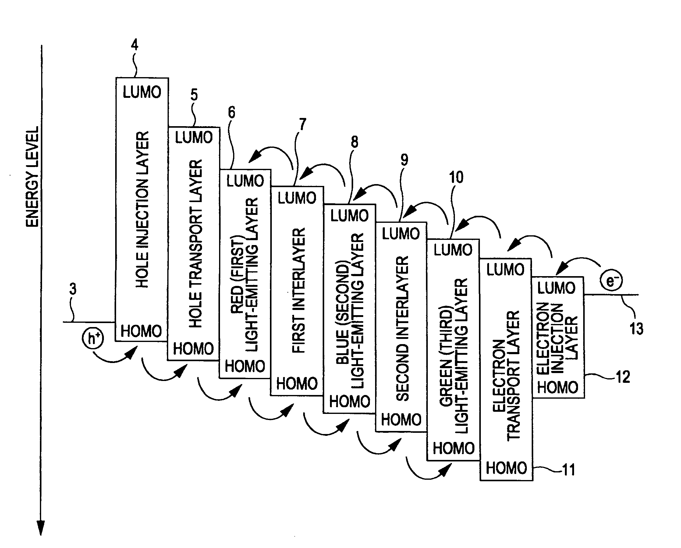
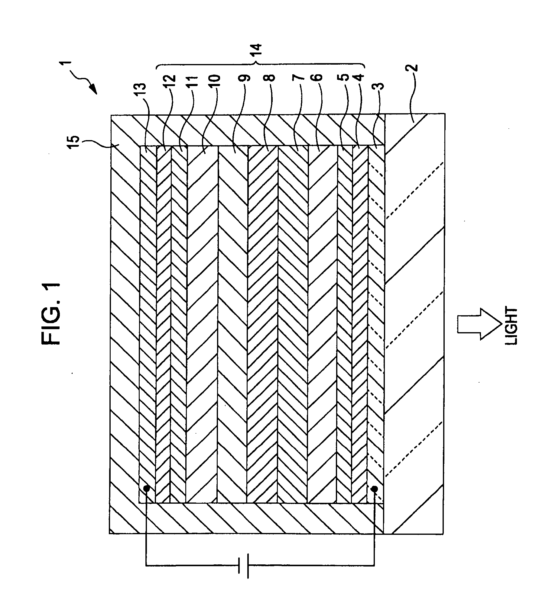
[0038]FIG. 1 is a schematic longitudinal cross-sectional view of a light-emitting element according to a first embodiment of the invention. FIG. 2 is a drawing illustrating the energy level of each of layers of the light-emitting element shown in FIG. 1. Note that, for the convenience of a description below, the upper side in FIG. 1 is defined as “top”, and the lower side in FIG. 1 is defined as “bottom”.

[0039]A light-emitting element (electroluminescence element) 1 shown in FIG. 1 emits red (R) light, green (G) light, and blue (B) light, thereby emitting white light. The light-emitting element 1 includes an anode 3, a hole injection layer 4, a hole transport layer 5, a red-light-emitting layer (first light-emitting layer)6, a first interlayer 7, a blue-light-emitting layer (second light-emitting layer)8, a second interlayer 9, a green-light-emitting layer (third light-emitting layer) 10, an electron transport layer 11, an electron injection layer 12, and a cathode 13, which are lam...

second embodiment

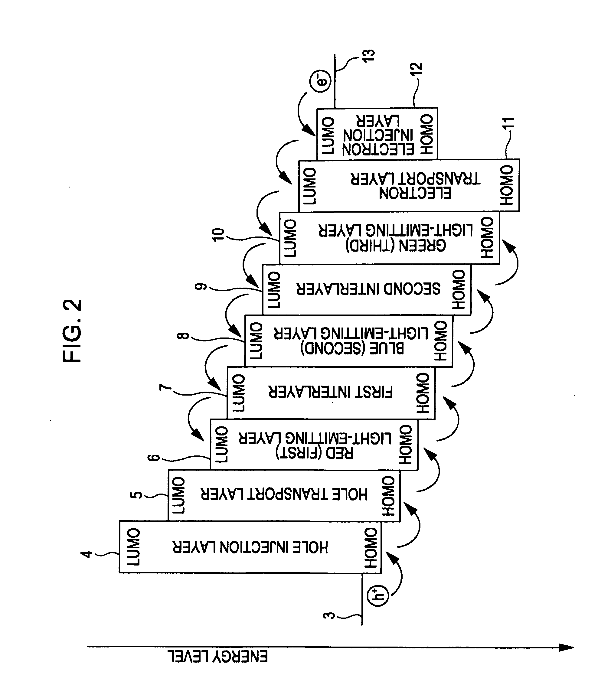
[0130]FIG. 3 is a schematic longitudinal cross-sectional view of a light-emitting element according to a second embodiment of the invention. FIG. 4 is a drawing illustrating the energy level of each of layers of the light-emitting element shown in FIG. 3. Note that, for the convenience of a description below, the upper side in FIG. 3 is defined as “top”, and the lower side in FIG. 3 is defined as “bottom”. A light-emitting element 1A of this embodiment is the same as the above-described light-emitting element 1 of the first embodiment except that the order of lamination of light-emitting layers is different, and each of a first interlayer and a second interlayer has a two-layer structure including a first layer and a second layer.

[0131]In the light-emitting element 1A of this embodiment, as shown in FIG. 3, a laminate 14A is interposed between an anode 3 and a cathode 13. In the laminate 14A, from the anode 3 side to the cathode 13 side, a hole injection layer 4, a hole transport la...

example 1

[0180](1) First, a transparent glass substrate having an average thickness of 0.5 mm was prepared. Next, an ITO electrode (anode) having an average thickness of 100 nm was formed on the substrate by sputtering. The substrate is then immersed in ethanol to perform ultrasonic cleaning. Subsequently, an oxygen plasma treatment was performed.

[0181](2) Next, CuPc was deposited by vacuum evaporation on the ITO electrode to form a hole injection layer having an average thickness of 20 nm.

[0182](3) Next, the above-mentioned amine hole transport material (α-NPD) represented by Chemical Formula 1 was deposited on the hole injection layer by vacuum evaporation to form a hole transport layer having an average thickness of 40 nm.

[0183](4) Next, a material of a green-light-emitting layer was deposited on the hole transport layer by vacuum evaporation to form the green-light-emitting layer (first light-emitting layer) having an average thickness of 10 nm. Regarding the material of the green-light-...


PUM


Abstract

A light-emitting element includes a cathode, an anode, a first light-emitting layer that is disposed between the cathode and the anode and that emits light of a first color, a second light-emitting layer that is disposed between the first light-emitting layer and the cathode and that emits light of a second color different from the first color, a third light-emitting layer that is disposed between the second light-emitting layer and the cathode and that emits light of a third color different from the first color and the second color, a first interlayer that is disposed between the first light-emitting layer and the second light-emitting layer so as to be in contact with the first and second light-emitting layers and that has a function of preventing energy transfer of an exciton between the first light-emitting layer and the second light-emitting layer, and a second interlayer that is disposed between the second light-emitting layer and the third light-emitting layer so as to be in contact with the second and third light-emitting layers and that has a function of preventing energy transfer of an exciton between the second light-emitting layer and the third light-emitting layer, wherein the first interlayer has a hole-transporting property higher than that of the second interlayer, and the second interlayer has an electron-transporting property higher than that of the first interlayer.

Description

BACKGROUND[0001]1. Technical Field[0002]The present invention relates to a light-emitting element, a display device, and an electronic apparatus.[0003]2. Related Art[0004]An organic electroluminescence element (organic EL element) is a light-emitting element having a structure in which at least one luminescent organic layer is interposed between an anode and a cathode. In such a light-emitting element, by applying an electric field between the cathode and the anode, an electron is injected into a light-emitting layer from the cathode side and a hole is injected into the light-emitting layer from the anode side. The electron and the hole are recombined in the light-emitting layer to generate an exciton. When the exciton returns to the ground state, a corresponding amount of energy is emitted as light.[0005]A known example of such a light-emitting element is an element which includes three laminated light-emitting layers corresponding to three colors of red (R), green (G), and blue (B...

Claims


Application Information

Patent Timeline
Patent Type & Authority Applications(United States)
IPC IPC(8): H01L33/00G09F9/30H01L27/32H01L51/50H05B33/12
CPCH01L51/5044H01L51/5096H05B33/14H05B33/10H01L2251/552H10K50/131H10K50/18H10K2101/30
Inventor YASUKAWA, KOJIMITSUYA, MASAYUKI
Owner INTELLECTUAL KEYSTONE TECH LLC
Why Eureka
Try Eureka