
Sputtering Method and Sputtering Apparatus, and Electronic Device Manufacturing Method

Inactive Publication Date: 2009-10-29
CANON ANELVA CORP
View PDF6 Cites 5 Cited by
  • Summary
  • Abstract
  • Description
  • Claims
  • Application Information

AI Technical Summary

Benefits of technology

[0018]According to the first aspect of the present invention, a plurality of targets are disposed efficiently and appropriately, so that processing variations and characteristic variations due to plasma nonuniformities that occur particularly at the center and end of a substrate can be suppressed. Therefore, according to the present invention, a substrate can be processed uniformly in the processing space.

Problems solved by technology

Hence, the above patent document does not sufficiently solve the problem of space reduction of the sputtering apparatus and the problem of a high throughput including the stability of the deposition conditions.

Method used


Image

  • Sputtering Method and Sputtering Apparatus, and Electronic Device Manufacturing Method
  • Sputtering Method and Sputtering Apparatus, and Electronic Device Manufacturing Method
  • Sputtering Method and Sputtering Apparatus, and Electronic Device Manufacturing Method

Examples


first embodiment

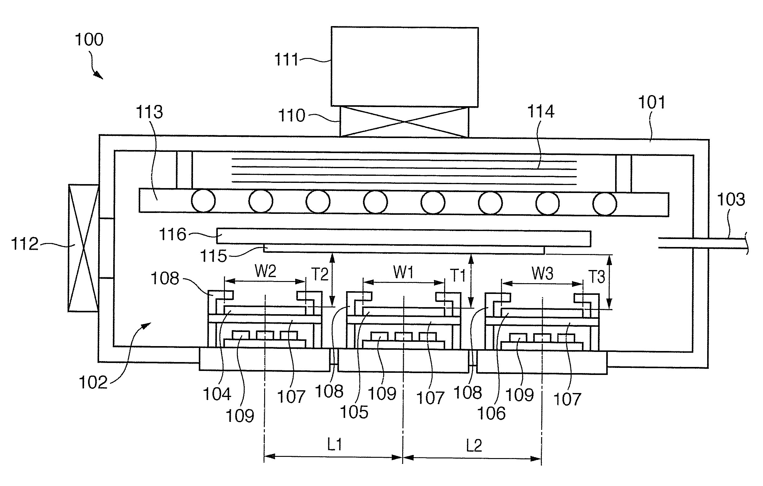
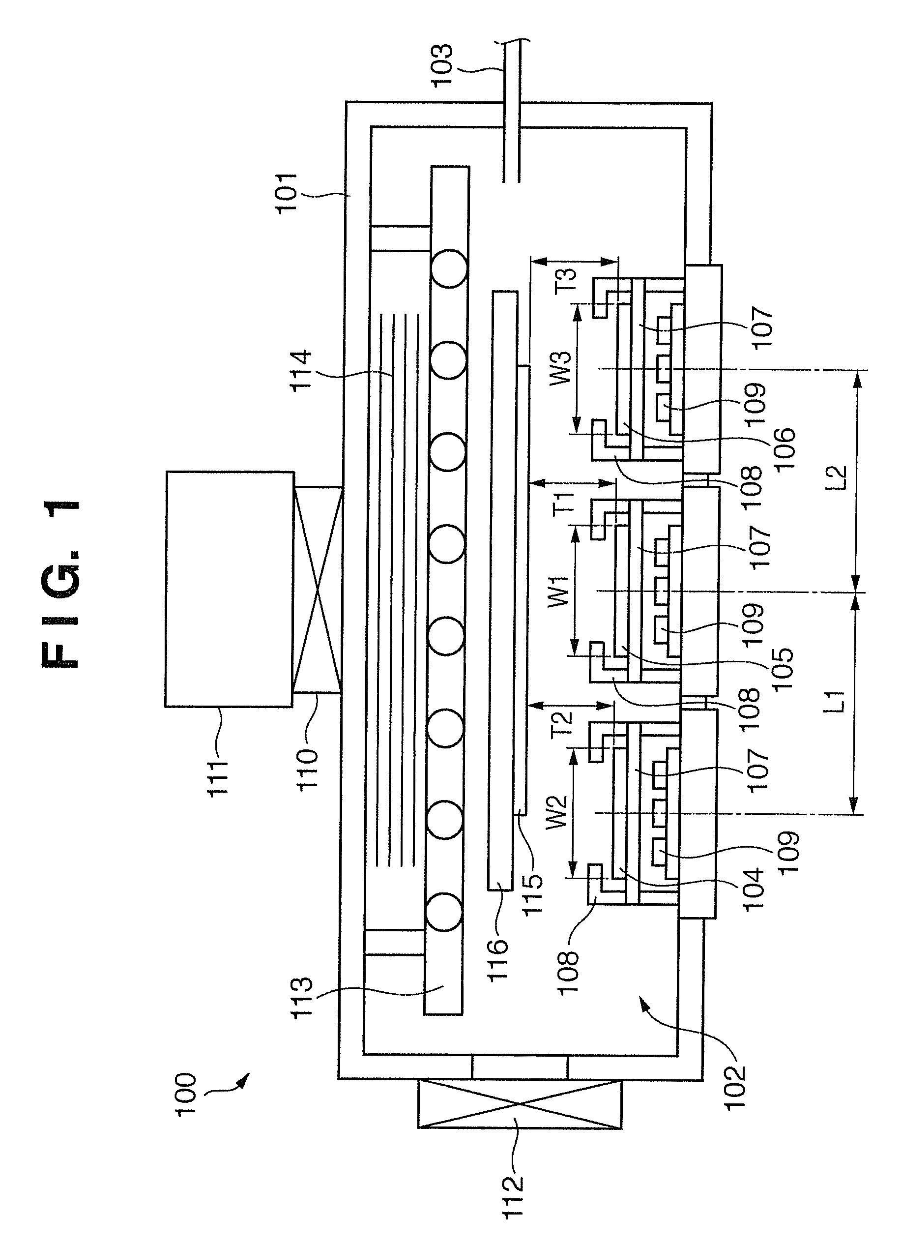
[0027]FIG. 1 is a schematic view showing an arrangement in which, as an example of a sputtering apparatus of this embodiment, three targets are arranged.

[0028]As shown in FIG. 1, a sputtering apparatus 100 includes a vacuum container 101 incorporating a processing chamber 102 serving as a processing space. First, second, and third targets 104, 105, and 106 are arranged in the processing chamber 102. A deposition target substrate 115 serving as a substrate and a substrate holder 116 for holding the deposition target substrate 115 are arranged in the processing chamber 102. The deposition target substrate 115 is transported within the processing chamber 102 in the vacuum container 101 at a predetermined speed.

[0029]The vacuum container 101 is connected to a vacuum pump 111 through an exhaust vale 110, and provided with a gas inlet port 103 and substrate inlet valve 112.

[0030]In the vacuum container 101, each of the targets 104, 105, and 106 is provided with a backing plate 107, deposi...

second embodiment

[0046]A continuous sputtering apparatus employing a roll-to-roll method will be described as the second embodiment. FIG. 3 shows a schematic view of the continuous sputtering apparatus of this embodiment. In the second embodiment, the same members as those of the first embodiment described above are denoted by the same reference numerals for the sake of convenience, and a repetitive description will be omitted.

[0047]As shown in FIG. 3, a continuous sputtering apparatus 200 of this embodiment continuously sputters a band-like substrate 201 as a belt-like long substrate. In the continuous sputtering apparatus 200, a vacuum container 101 is connected to a feed container 202 and take-up container 203 for the band-like substrate 201 through gas gates 205.

[0048]The feed container 202 has a feed bobbin 206 for feeding the band-like substrate 201. The take-up container 203 has a take-up bobbin 207 for taking up the band-like substrate 201. In each of the feed container 202 and take-up conta...


PUM

PropertyMeasurementUnit
Ratioaaaaaaaaaa

Abstract

A sputtering method comprising the steps of: arranging the plurality of targets in a vacuum container equidistantly in a transport direction of the substrate such that distances between the plurality of rectangular targets and the substrate are different; and assuming that lengths of sides, parallel to the transport direction, of adjacent first and second targets are expressed as first and second target width W1 and W2, respectively, and that a gap between the first and second targets is expressed as L, when a relationship among the first target width W1, the second target width W2, and the gap L satisfies L≦3(W1+W2), and assuming that a distance from each of the plurality of targets to the substrate is expressed as T, performing sputtering such that a relationship between a longest distance Tmax and the gap L at this time satisfies 0.4≦Tmax / L≦0.8.

Description

BACKGROUND OF THE INVENTION[0001]1. Field of the Invention[0002]The present invention relates to a sputtering method and sputtering apparatus for forming a film on a substrate by sputtering, and an electronic device manufacturing method to manufacture, for example, a photovoltaic element using amorphous silicon (a-Si) on a glass substrate.[0003]2. Description of the Related Art[0004]Conventionally, the manufacture of a photoelectric conversion device such as a solar cell and the manufacture of a flat panel display (the photoelectric conversion device and flat display panel will be generically referred to as an electronic device hereinafter) generally widely employ a sputtering apparatus. Particularly, as a method of manufacturing a solar cell, the following technique is known.[0005]For example, in a manufacturing process for a solar cell using a non-single-crystal semiconductor film or the like, plasma CVD (Chemical Vapor Deposition) is generally employed for forming the non-single-...

Claims


Application Information

Patent Timeline
IPC IPC(8): C23C14/34
CPCC23C14/086C23C14/562C23C14/3464
Inventor HORI, TADASHI
Owner CANON ANELVA CORP
Learn More