I/O Driver For Integrated Circuit With Output Impedance Control

a technology of output impedance control and driver, which is applied in logic circuits, pulse techniques, and increasing the modification of reliability, etc., can solve the problems of significant deviation of output impedance response, unsatisfactory signal degradation, and mismatched impedance, so as to improve the linearity of output impedance or voltage/current (v/i) output characteristics, and enhance esd protection

Active Publication Date: 2009-10-29
MARVELL ASIA PTE LTD
View PDF2 Cites 18 Cited by
  • Summary
  • Abstract
  • Description
  • Claims
  • Application Information

AI Technical Summary

Benefits of technology

[0009]The I / O driver circuit of the invention controls I / O output impedances using a combination of FET pull-up and pull-down stages in series with a linear resistive element. The pull-up and pull-down stages include respective PFET and NFET arrays, which are controlled to exhibit predefined conductances by a logical circuit and respective pull-up and pull-down calibration words. The combined programmed conductance values in the active PFET and NFET devices operate to better maintain output impedance or voltage / current (v / i) output characteristic linearity for the entire switching period, whether transitioning from a first to a second voltage level, or transitioning from the second to the first voltage level. For that matters the NFETS are arranged in a stack of at least two NFETs in order to provide enhanced ESD protection.

Problems solved by technology

The signal reflections result in undesirable signal degradation.
Mismatched impedance can occur for any number of reasons.
The problem is acute at switching, where the output impedance response can vary significantly as the output signal (at the pad) transitions between voltage levels.
Unfortunately, the output impedance is often linear only over a small range of the output voltage, so a calibrated output does not overcome the problem of fluctuating output impedance for the entire voltage switching range.
For that matter, due to the non-linear nature of the FET array operation at the time of switching, the output impedance over the different stages of the switching period can still vary undesirably.

Method used


Image

  • I/O Driver For Integrated Circuit With Output Impedance Control
  • I/O Driver For Integrated Circuit With Output Impedance Control
  • I/O Driver For Integrated Circuit With Output Impedance Control

Examples


Embodiment Construction

[0014]Reference will now be made in detail to the present invention, examples of which are illustrated in the accompanying drawings, wherein like reference numerals refer to like elements throughout.

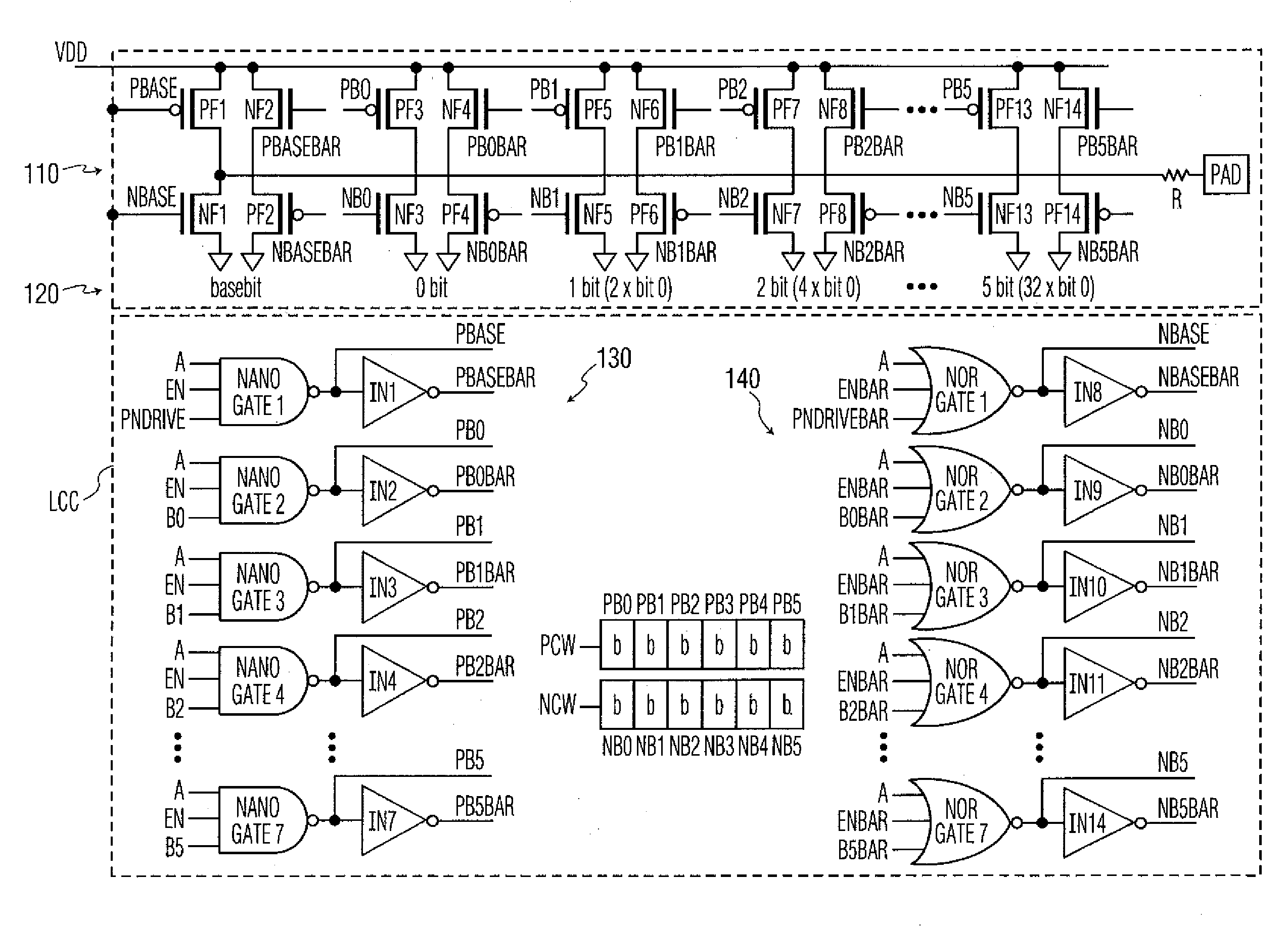
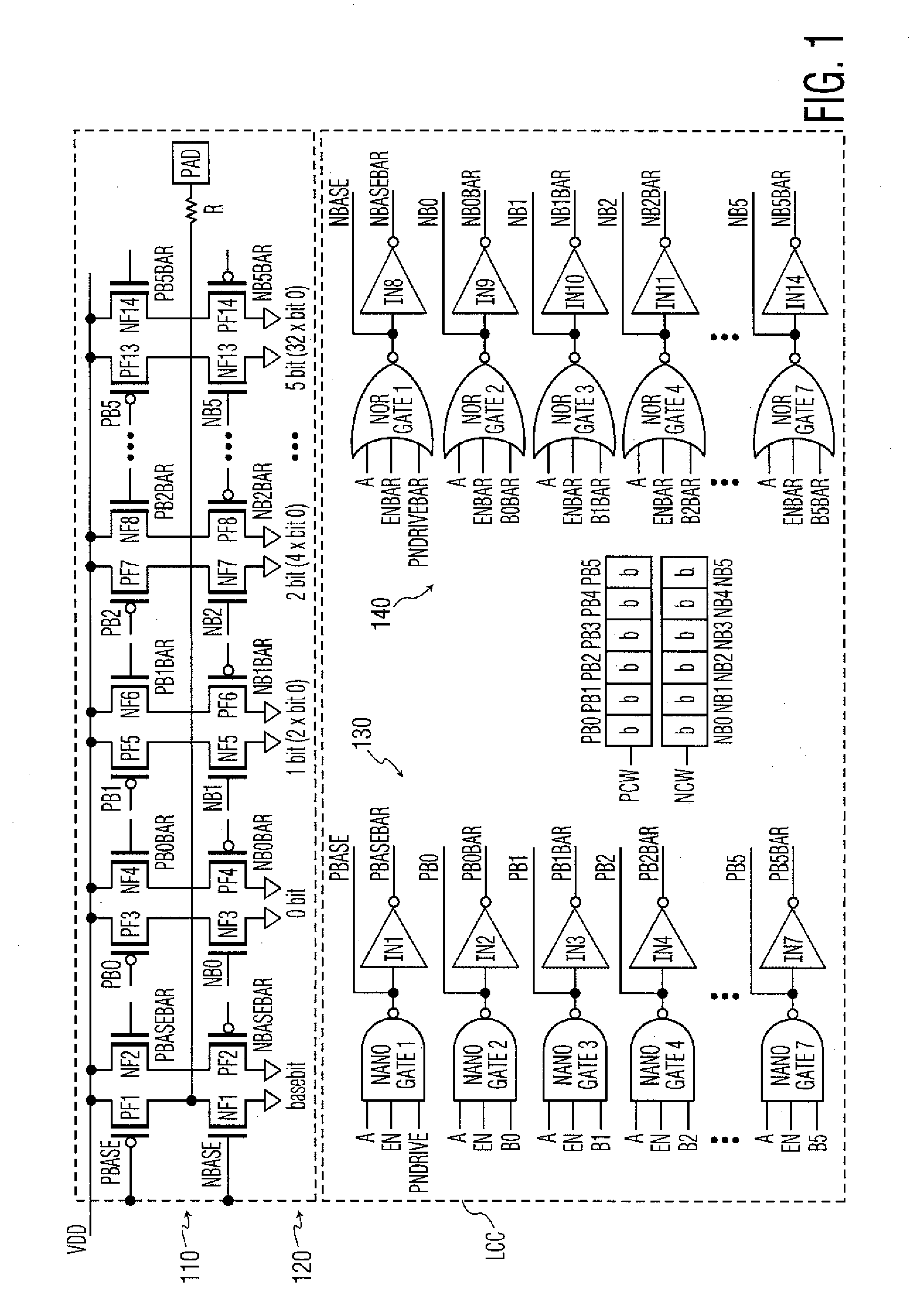
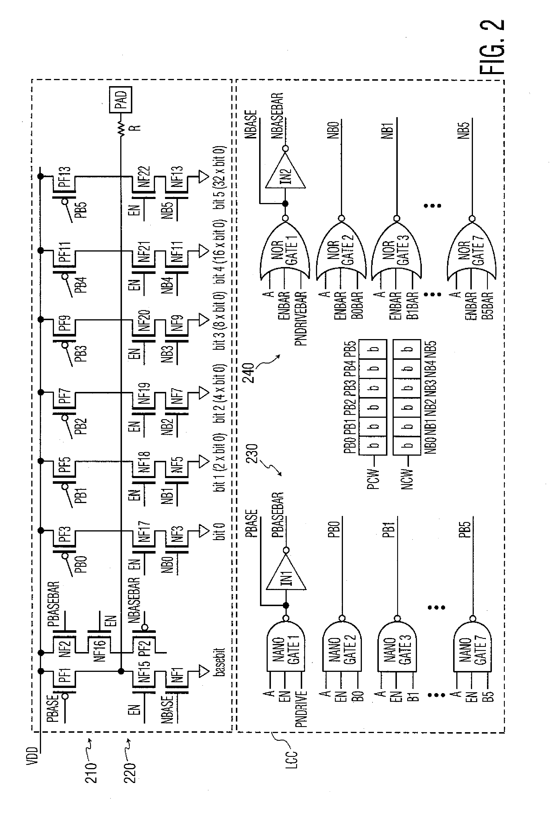
[0015]FIG. 1 shows one embodiment of an I / O driver with output impedance control for maintaining a substantially flat output impedance response. The I / O driver may be described as a transmission gate configuration. The configuration comprises a resistive element (R), connected between an active impedance matching element and an I / O output pad (PAD). The active impedance matching element is controlled by a logical control circuit (LCC). The logical control circuit (LCC) receives a data signal A comprising a time series of voltage state transitions, e.g., between logic one and logic zero, representative of digital I / O data, enable signals EN and PNDRIVE and calibration control words PCW and NCW. Calibration control words PCW and NCW control respective PFET pull-up (e.g., to VDD) and NFET p...


PUM


Abstract

An I / O driver has v / i characteristic control for maintaining a substantially flat output impedance response using a transmission gate configuration at an I / O output pad. The configuration includes a linear resistive element electrically connected at an I / O pad for limiting a processed data I / O signal, an active impedance element for receiving and processing the data signal, which comprises data represented by a series of voltage state transitions, and pull-up and pull-down array calibration words, for generating and outputting a processed I / O output signal to the resistive element to output a substantially flat v / i response at switching of the data signal.

Description

[0001]The present invention relates broadly to I / O drivers for integrated circuits (ICs), and more directly to I / O drivers for improving output impedance response during switching.BACKGROUND[0002]Integrated circuits (ICs) send signals outside of the IC circuitry using output driver circuits or drivers. Input / output (I / O) drivers present signals to output signal pads, which connect to a pin, the set of pins referred to as the packaging. The pin or packaging connects to a trace or bus. The signal pad displays inherent parasitic resistance, inductance, and capacitance (sometimes referred to as the characteristic package impedance). The characteristic package impedance affects transmission of the output signal from the signal pad (i.e., the IC). The trace in receipt of the output signal displays transmission line characteristics: resistance, capacitance and inductance (sometimes referred to as the characteristic impedance). The characteristic impedance also affects transmission of the o...

Claims


Application Information

Patent Timeline
Patent Type & Authority Applications(United States)
IPC IPC(8): H03K19/003
CPCH03K19/0005
Inventor CHEN, DAVID JIALAWSON, WILLIAM FREDERICKMANN, DAVID WILLIAM
Owner MARVELL ASIA PTE LTD
Why Eureka
Try Eureka