Drive Circuit, Display Device Provided With Such Drive Circuit and Method for Driving Display Device

a drive circuit and display device technology, applied in the direction of digital storage, instruments, computing, etc., can solve the problems of large through current problem, increase in power consumption of the circuit, and high frequency noise generation in the power source line, so as to suppress the increase in power consumption and prevent the race hazard of the shift register. , the effect of overlapping the input signal of the flip-flop

Active Publication Date: 2009-10-29
SHARP KK
View PDF5 Cites 17 Cited by
  • Summary
  • Abstract
  • Description
  • Claims
  • Application Information

AI Technical Summary

Benefits of technology

[0052]Therefore, a through current does not flow in each logical derivation stage of the MOS type logical operation circuit, while the output signal of the flip-flop is inactive. The through current is a current which flows by being effected by a plurality of logical derivation paths which are conductive at the same time in accordance with the periodic level change of the first clock signal and the second clock signal. If the logical operation circuit is used for preventing the race hazard of the sh

Problems solved by technology

The flowing of the through current causes a problem of the increase in power consumption by the circuit which includes the through current generating part, regardless of the race hazard preventing circuit 22.
In addition, the flowing of the through current causes another problem that a high frequency noise generates in the power source line.
This causes the pr

Method used


Image

  • Drive Circuit, Display Device Provided With Such Drive Circuit and Method for Driving Display Device
  • Drive Circuit, Display Device Provided With Such Drive Circuit and Method for Driving Display Device
  • Drive Circuit, Display Device Provided With Such Drive Circuit and Method for Driving Display Device

Examples


first embodiment

[0085]One embodiment of the present invention is described below with reference to FIGS. 1 through 5.

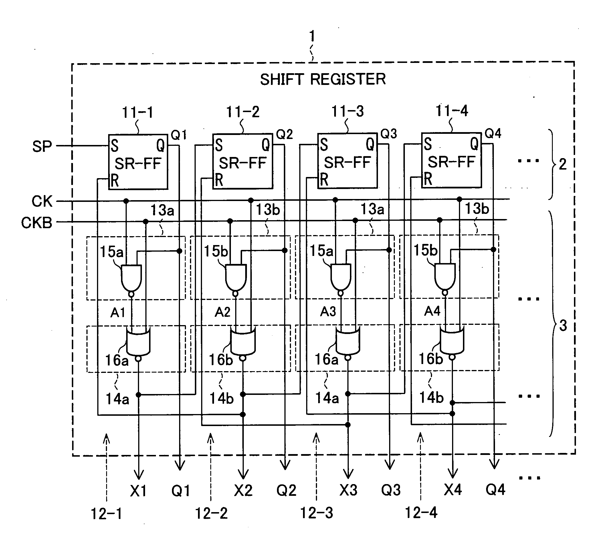
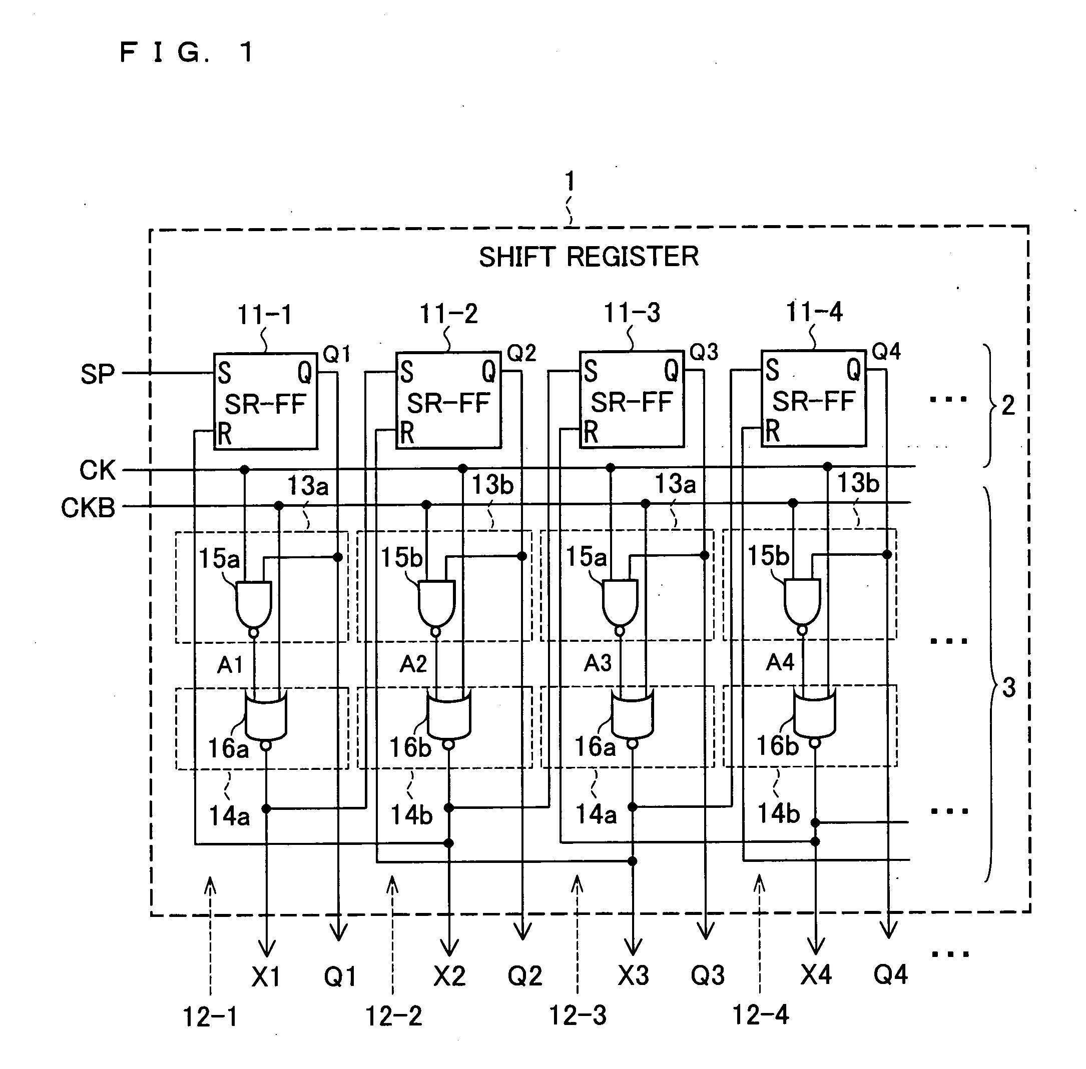
[0086]FIG. 1 illustrates an arrangement of a shift register 1 pertaining to the present embodiment. In the embodiment, it is assumed that a display data is inputted to a display panel such as a liquid crystal panel, by using the shift register 1. The shift register 1 is connected to a level shifter, an analog switch, and other components. The level shifter performs level shifting of an output signal, and the analog switch is driven by an output signal of the level shifter. The driving circuit of the display device which includes the display panel may indicate a driving circuit which is solely made from the level shifter 1, or may indicate the whole of the driving circuit including the other circuits such as the level shifter and the analog switch to be connected to the level shifter 1.

[0087]The stage numerals of the shift register 1 are consecutively 1, 2, 3, . . . from the first sta...

second embodiment

[0146]The following description deals with another embodiment of the present invention, with reference to FIGS. 6 through 11. Unless explained otherwise, members with the same reference numerals as what are explained in First Embodiment have the same function.

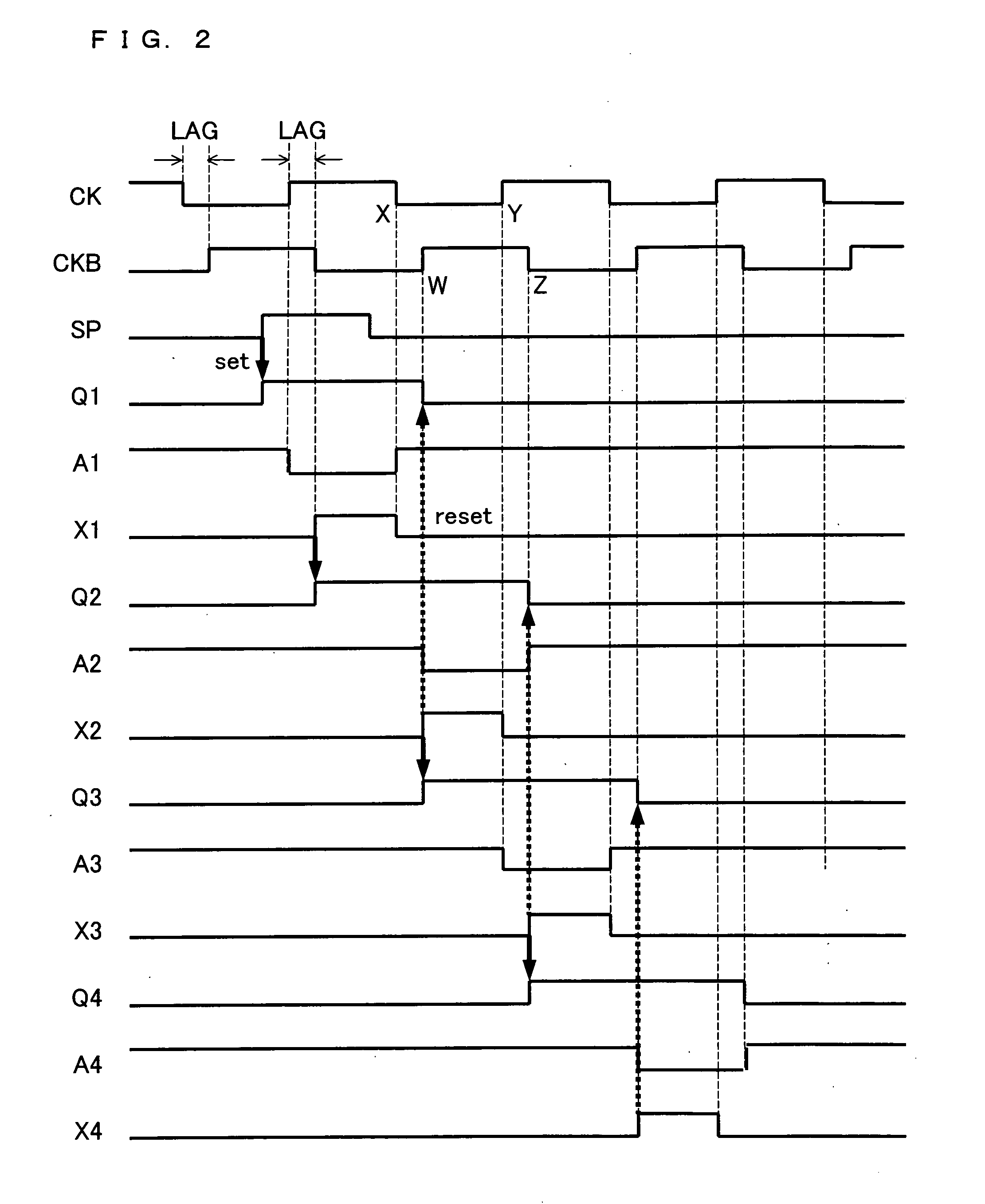
[0147]Race hazard may occur in the arrangement of FIG. 1 of First Embodiment, if a rising and decaying exponential of a waveform of the clock signals CK and CKB is large, and a difference exists in the logic threshold value between the logic gates such as between the NAND circuits 15a and 15b and the NOR circuits 16a and 16b. FIGS. 6(a) through 6(c) illustrate what kind of effect the High and Low of a clock signal CKnand and the High and Low of a clock signal CKnor give to the output signals X, Q and A, when the waveform of the clock signal CK is risen or decayed, and a difference exists between the logical threshold value V THnand of the NAND circuits 15a and 15b and the logical threshold value V THnor of the NOR circuits 16a ...


PUM


Abstract

While an output signal of a flip-flop is inactive in a shift register, NAND circuits of clock pulse extracting sections prevent the performing of conduction switching operation in accordance with periodic level change of clock signals between a logical derivation path for High output and a logical derivation path for Low output, by input of the output signal.

Description

TECHNICAL FIELD[0001]The present invention relates to a driving circuit which drives a display panel of a liquid crystal display device or the like.BACKGROUND ART[0002]A liquid crystal display device includes a source driver circuit and a gate driver circuit as driving circuits for driving a display panel. For these driving circuits, a shift register is used for generating a drive signal which controls a drive timing of the display panel. An example of such a shift register is illustrated in FIG. 12.[0003]A shift register 101 as illustrated in FIG. 12 includes a set / reset type flip-flop 102 (102-1, 102-2, . . . ) and a CMOS analog switch 103 (103-1, 103-2, . . . ) in each stage. In addition, the shift register 101 is arranged so that it receives a start pulse SP and two clock signals CK and CKB. The two clock signals CK and CKB have different phases to each other.[0004]The set / reset type flip-flop (hereafter referred as ‘flip-flop’) 102 is set by receiving an active set signal at an...

Claims


Application Information

Patent Timeline
IPC IPC(8): G09G5/00G11C19/00
CPCG09G3/3677G09G3/3688G11C19/28G09G2330/021G11C19/00G09G2310/0286
Inventor SHIMIZU, SHINSAKUMURAKAMI, YUHICHIROH
Owner SHARP KK
Why Eureka
Try Eureka