

Image sensor, imaging system, and image sensor control method
- Summary
- Abstract
- Description
- Claims
- Application Information
AI Technical Summary
Benefits of technology
Problems solved by technology
Method used
Image

Examples
first embodiment
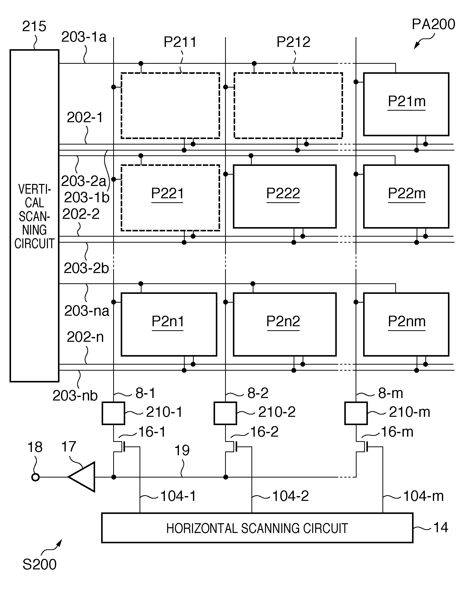
[0130]A pixel P311 in the pixel array PA300 is different from the pixel P211 in the first embodiment in that the drain of a reset MOS transistor 304 is connected to a column signal line 8-1. The arrangements of remaining pixels P312 to P3nm are also equivalent to that of the pixel P311.
[0131]The noise reduction circuit 310-1 is different from the noise reduction circuit 210-1 in the first embodiment in that the noise reduction circuit 310-1 includes a power supply switching circuit (voltage supply unit) 320 instead of the voltage supply unit 213. The arrangements of the remaining noise reduction circuits 310-2 to 310-m are also equivalent to that of the noise reduction circuit 310-1.
[0132]The power supply switching circuit320 is connected to the column signal line 8-1 via a power supply line SL300. The power supply switching circuit 320 includes switches 311 and 312. When the switch 311 is turned on and the switch 312 is turned off, the first electric potential (e.g. a power supply ...
third embodiment
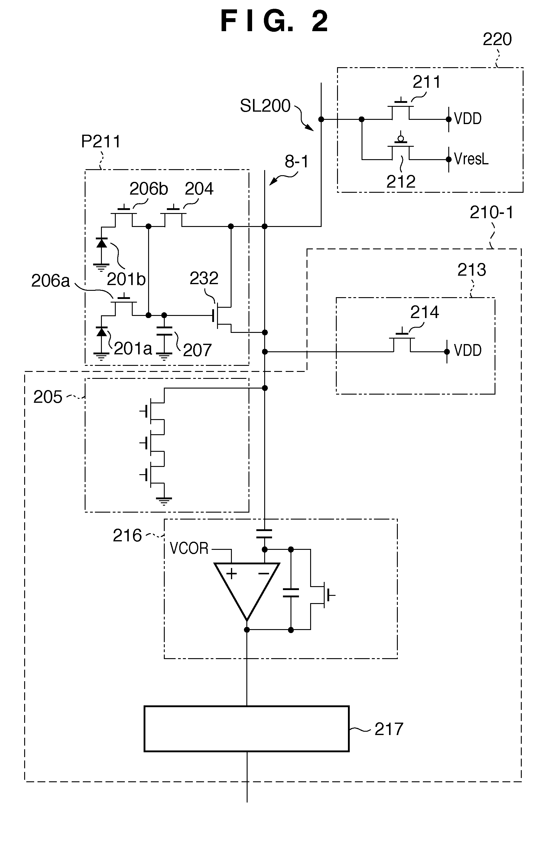
[0142]To solve this problem, in the third embodiment, the times during which the pulses PTN and PTS are at H level are shortened. In addition, a signal of one pixel is sampled a plurality of number of times at short intervals.
[0143]For example, in a second period TP21 between timings T6 and T52 shown in FIG. 5, the pulse PSB has changed to L level. In the second period TP21, a switch 214 is turned off, and a voltage supply unit 213 has stopped a supply operation of the set voltage (e.g. a power supply voltage VDD) to a column signal line 8-1. The pulse PVLON has changed to H level. In the second period TP21, while the electric potential of an FD in a selected pixel is maintained at the electric potential (first electric potential) of the selected state, an amplification MOS transistor in the pixel is turned on.
[0144]In the second period TP21, the pulse PTN changes to H level at a timing immediately after an amplification MOS transistor 232 in the pixel on the selected row is turned ...
PUM
 Abstract
Description
Claims
Application Information