Semiconductor device

a technology of semiconductors and devices, applied in the direction of resistance/reactance/impedence, testing circuits, instruments, etc., can solve the problems of increasing testing costs, and achieve the effects of reducing the number of connecting signal lines, low cost, and efficient testing of sip

Inactive Publication Date: 2009-10-29
RENESAS ELECTRONICS CORP
View PDF3 Cites 5 Cited by
  • Summary
  • Abstract
  • Description
  • Claims
  • Application Information

AI Technical Summary

Benefits of technology

[0012]A representative test method for an SiP configured from a plurality of LSI chips includes performing adequate testing on each of the chips before assembly to form the SiP, and testing connectivity between each chip after assembly. At this time, in cases where there are components that cannot adequately be tested in a chip state, by giving consideration at a chip design stage to a circuit that enables testing of the SiP and to reducing the number of connecting signal lines between each chip, it is possible to test the SiP efficiently and at low cost.
[0013]According to a conventional configuration it is possible to reduce the number of data bus signal lines. However, when in a test mode, in the device disclosed in Patent Document 1, a high multiplier clock signal is necessary. Moreover, in the device disclosed in Patent Document 2, it is necessary to operate with a clock signal at both a H level and an L level. As a result, a high performance LSI tester, in which special conditions are required in a test clock signal, is necessary, and the cost of testing increases.

Problems solved by technology

As a result, a high performance LSI tester, in which special conditions are required in a test clock signal, is necessary, and the cost of testing increases.

Method used


Image

  • Semiconductor device
  • Semiconductor device

Examples


first exemplary embodiment

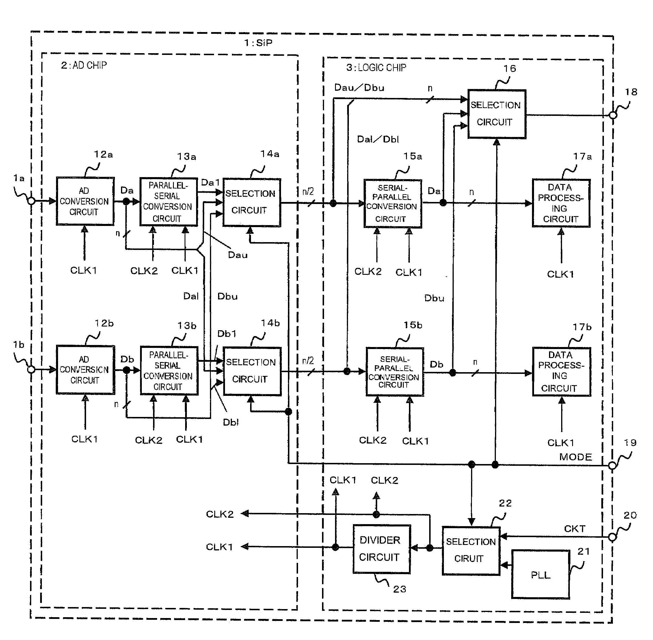
[0028]FIG. 1 is a block diagram showing a configuration of a semiconductor device according to a first exemplary embodiment of the present invention. In FIG. 1, the semiconductor device is an SiP 1 in which an AD chip 2, that has 2 channel AD conversion circuits, and a logic chip 3 are included on one package. The SiP 1 is provided with terminals 11a and 11b that receive analog signals, a terminal 18 for test output, a terminal 19 for a test mode selection, and a terminal 20 for receiving a test clock signal.

[0029]The AD chip 2 is provided with AD conversion circuits 12a and 12b, parallel-serial conversion circuits 13a and 13b, and selection circuits 14a and 14b. The logic chip 3 is provided with serial-parallel conversion circuits 15a and 15b, selection circuits 16 and 22, data processing circuits 17a and 17b, a PLL 21, and a divider circuit 23.

[0030]The AD chip 2 receives analog signals from the terminals 11a and 11b, and receives a selection clock CLK2, a clock signal CLK1 that i...


PUM


Abstract

Cost of testing is reduced. An SiP (1) comprises an AD chip (2) and a logic chip (3) that perform transmission and reception of data. The AD chip (2) comprises AD conversion circuits (12a and 12b) that generate parallel data, parallel-serial conversion circuits (13a and 13b) that divide parallel data generated by the AD conversion circuits (12a and 12b) and perform time-based sorting, and selection circuits (14a and 14b) that select any of: output data of the parallel-serial conversion circuits (13a and 13b), or divided data obtained by dividing the parallel data so as to enable transmission of each thereof by said plural paths, and output to the logic chip (3). The logic chip (3) comprises serial-parallel conversion circuits (15a and 15b) that recover original parallel data from data sorted in a time-based manner, and a selection circuit (16) that selects: original parallel data obtained by combining the divided data, or original parallel data recovered by the serial-parallel conversion circuits (15a and 15b), and outputs to a terminal (18).

Description

REFERENCE TO RELATED APPLICATION[0001]This application is based upon and claims the benefit of the priority of Japanese patent application No. 2008-117432, filed on Apr. 28, 2009, the disclosure of which is incorporated herein in its entirety by reference thereto.TECHNICAL FIELD[0002]The present invention relates to a semiconductor device, and in particular, to test technology for a semiconductor device in which a plurality of LSI chips are mounted on one package.BACKGROUND[0003]In recent years, in semiconductor packages, technologies in which a plurality of LSI chips is included in one package, such as SiP (System in Package) and MCP (Multi Chip Package), are attracting attention. Along with significant development and growth of electronic information devices, digital domestic electrical appliances, and the like, there is increasing demand for more multi-functionality and high performance in LSIs, so that attention is being focused upon SoC (System on Chip) technology that realizes...

Claims


Application Information

Patent Timeline
Patent Type & Authority Applications(United States)
IPC IPC(8): G06F19/00G01R31/28H01L21/822H01L27/04
CPCG01R31/31726H01L2924/0002H01L2924/00G11C29/00
Inventor TASHIRO, YASUNORI
Owner RENESAS ELECTRONICS CORP
Why Eureka
Try Eureka