Light-emitting diode package assembly

a technology of light-emitting diodes and package assemblies, which is applied in the direction of semiconductor devices for light sources, light-emitting devices, solid-state devices, etc., can solve the problems of limited operating current, design limits of devices and materials, and care must be exercised, so as to improve the light-emitting diodes.

Active Publication Date: 2009-11-12
FJELSTAD JOSEPH CHARLES
View PDF10 Cites 45 Cited by
  • Summary
  • Abstract
  • Description
  • Claims
  • Application Information

AI Technical Summary

Benefits of technology

[0032]Accordingly, it is an object of the present invention to provide improved light emitting diode (LED) package assemblies.

Problems solved by technology

In the operation of a LED the luminous intensity is roughly proportional to the amount of current that is supplied, and the higher the current the greater will be the light intensity produced, subject to the design limits of the device and the materials used.
Care must be exercised, however, as the operating current often must be limited relative to the amount of heat in the application.
Similarly, LEDs designed to operate at higher voltages are subject to greater heat.
The use of solders and higher temperature soldering processes, however, are rife with problems.
These materials and processes have always had certain disadvantages, and a number of new trends in the electronics industry as well as newly emerging applications for LEDs are revealing or exacerbating other disadvantages, especially for arrays and other assemblies containing many LEDs.
One set of such disadvantages relates to solder materials.
Unfortunately, both tin and especially lead have serious chemical disadvantages.
For these two metals, mining the ores, refining those ores, working with the refined metals during manufacturing, being exposed to substances including these in manufactured products, and disposing of the products at the ends of their life cycles are all potentially damaging to human and animal health and to the environment.
Mining, refining, working during manufacturing, exposure from manufactured products, and disposal are still all issues for tin, silver, and copper.
Furthermore, SAC solder processes are prone to other problems, such as the formation of shorts (e.g., “tin whiskers”) and opens if surfaces are not properly prepared.
It follows that the undue use of some materials, like those in solders, are generally undesirable in electronic assemblies, including LED assemblies.
Another set of disadvantages in the solder-based assembly of electronic products is the high temperature processes that are inherently required.
The use of heat on and around many electronic components has always been undesirable.
As a general principle, the heating of electronic components increases their failure rate in later use and beyond a certain point outright destroys such components.
When SAC type solders are used the likelihood of component damage is much higher, resulting in assemblies that fail during post-manufacturing testing as well as in-the-field failures.
Additionally, generating and managing the heat during manufacturing have increased energy, safety, and other costs.
It therefore follows that the undue use of heat-based manufacturing processes, like soldering, is also generally undesirable in electronic assemblies.
Increasingly yet another set of disadvantages in the solder-based assembly of electronic products is one related to the “adding” of materials.
Solders contain higher density metals, thus increasing the ultimate weight of electronic products.
Liquid solders have high surface tensions and effects from this also usually require major design consideration.
Accordingly, it further follows that the undue use of any additional material in manufactured assemblies and in manufacturing processes, again like solder, is generally undesirable in the resulting electronic assemblies.
In addition to the noted disadvantages in the solder-based assembly of electronic products, generally, there can be additional problems in particular in the solder-based assembly of LEDs.
For example, in a LED the soldering process can be difficult because the ideal substrates for thermal degradation protection are typically good thermal conductors, purposefully being used because they have a high thermal capacity that will help keep the LED assembly within in desired temperature range during operation.
This creates a significant challenge for solder assembly of LED packages, however, because the package must be raised to an even more elevated temperature to create reliable solder joints and the necessary temperatures can then degrade or damage the encapsulant used in the manufacture of the LED package.
Moreover, exposure to certain cleaning chemicals may attack the LED surface and cause discoloration.
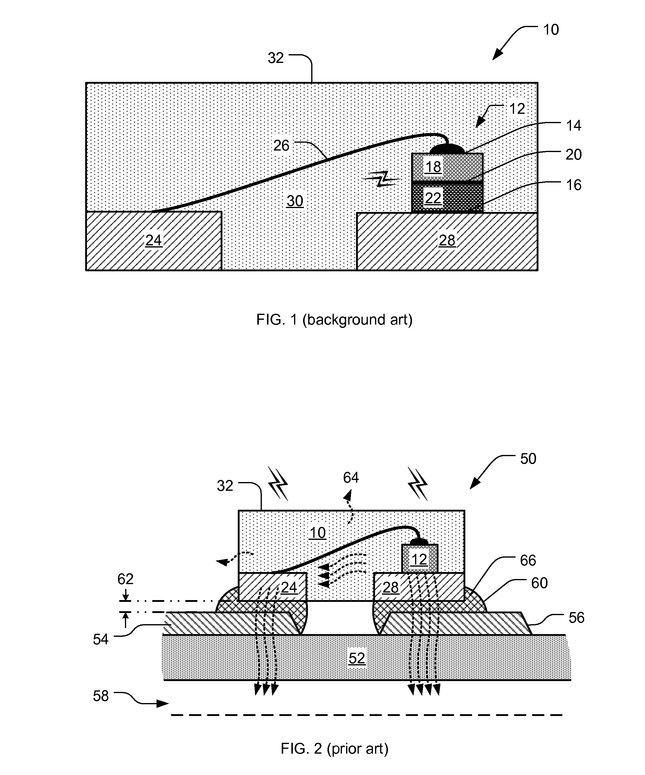
The substrate 52 will typically serve to some extent to transfer heat, but it may not be optimal for that.
In some applications this thermal flow can cause serious problems.
For instance, if too much heat builds up in the LED package 10 it may be damaged internally.
The solder pads 60 tend to be thermally conductive, but they nonetheless lengthen and complicate the primary paths that thermal energy must travel to exit the LED package 10.
Unfortunately however, the solder pads 60 tend to interfere with what can be done here.
In summary, the use of solder materials, the use of heat-based soldering manufacturing processes, the undue addition of solder material to manufactured assemblies and these and additional problems particular to the solder-based assembly of LEDs are all generally undesirable.

Method used


Image

  • Light-emitting diode package assembly
  • Light-emitting diode package assembly
  • Light-emitting diode package assembly

Examples


Embodiment Construction

[0050]A preferred embodiment of the present invention is a light emitting diode (LED) package assembly. As illustrated in the various drawings herein, and particularly in the view of FIGS. 3-10, preferred embodiments of the invention are depicted by the general reference character 100. A number of representative variations of LED package assemblies 100 in accord with the present invention are now described.

[0051]FIGS. 3a-e depict a series of stages in a process flow during manufacturer of a representative LED package assembly 100, 300 in accord with the present invention. [To differentiate from other variations of the LED package assembly 100, the variation in FIGS. 3a-e is referenced specifically as LED package assembly 300 and a similar convention is used throughout the following discussion.]

[0052]In FIG. 3a the LED package assembly 300 has a metal base 310, an insulator 312 coating on the top side of the base 310, and a continuous metal plating or foil 314 covering the top side o...


PUM


Abstract

An electrical device containing multiple light emitting diode (LED) dies each having respective first and second connectors suitable to receive current through the LED die. A common base layer of a first electrically conductive material has cavities into which at least one LED die is mounted with its second connector electrically connected by a conductive bonding material to the first conductive material of the base layer. One or more over-layer sections of a second electrically conductive material each are electrically connected by a bond to at least one of the first connector of a LED die. And an insulator electrically separates the first conductive material of the base layer from the second conductive material of over-layer sections.

Description

CROSS-REFERENCE TO RELATED APPLICATIONS[0001]This application claims the benefit of U.S. Provisional Application No. 60 / 052,592, filed May 12, 2008, hereby incorporated by reference in its / their entirety.STATEMENT REGARDING FEDERALLY SPONSORED RESEARCH OR DEVELOPMENT[0002]Not applicable.THE NAMES OF THE PARTIES TO A JOINT RESEARCH AGREEMENT[0003]Not applicable.INCORPORATION-BY-REFERENCE OF MATERIAL SUBMITTED ON A COMPACT DISC[0004]Not applicable.COPYRIGHT NOTICE AND PERMISSION[0005]This document contains some material which is subject to copyright protection. The copyright owner has no objection to the reproduction with proper attribution of authorship and ownership and without alteration by anyone of this material as it appears in the files or records of the Patent and Trademark Office, but otherwise reserves all rights whatsoever.BACKGROUND OF THE INVENTION[0006]1. Technical Field[0007]The present invention relates generally to light-emitting diode (LED) arrays and the assembly th...

Claims


Application Information

Patent Timeline
Patent Type & Authority Applications(United States)
IPC IPC(8): H01L33/00H01L21/00H01L33/62H01L33/64
CPCF21K9/00H01L25/0753H01L2924/12041H01L2224/92247H01L2224/83192H01L2924/01029H01L2224/73265H01L2224/48465H01L2224/48247H01L2224/32245H01L24/82H01L24/24H01L33/647H01L33/641H01L33/62H01L2224/48091H01L2924/00014H01L2924/00012H01L2924/00H01L2924/351H01L2924/12036H01L24/73H01L2924/15153
Inventor FJELSTAD, JOSEPH C.
Owner FJELSTAD JOSEPH CHARLES
Why Eureka
Try Eureka