NAND based NMOS NOR flash memory cell, a NAND based NMOS nor flash memory array, and a method of forming a NAND based NMOS NOR flash memory array

Inactive Publication Date: 2009-11-12
APLUS FLASH TECH
View PDF42 Cites 89 Cited by
  • Summary
  • Abstract
  • Description
  • Claims
  • Application Information

AI Technical Summary

Benefits of technology

[0024]An object of this invention is to provide a NOR flash nonvolatile memory device that provides the memory cells size and a low current

Problems solved by technology

One disadvantage of NOR flash nonvolatile memory is as the density is doubled, the number of its

Method used


Image

  • NAND based NMOS NOR flash memory cell, a NAND based NMOS nor flash memory array, and a method of forming a NAND based NMOS NOR flash memory array
  • NAND based NMOS NOR flash memory cell, a NAND based NMOS nor flash memory array, and a method of forming a NAND based NMOS NOR flash memory array
  • NAND based NMOS NOR flash memory cell, a NAND based NMOS nor flash memory array, and a method of forming a NAND based NMOS NOR flash memory array

Examples


Embodiment Construction

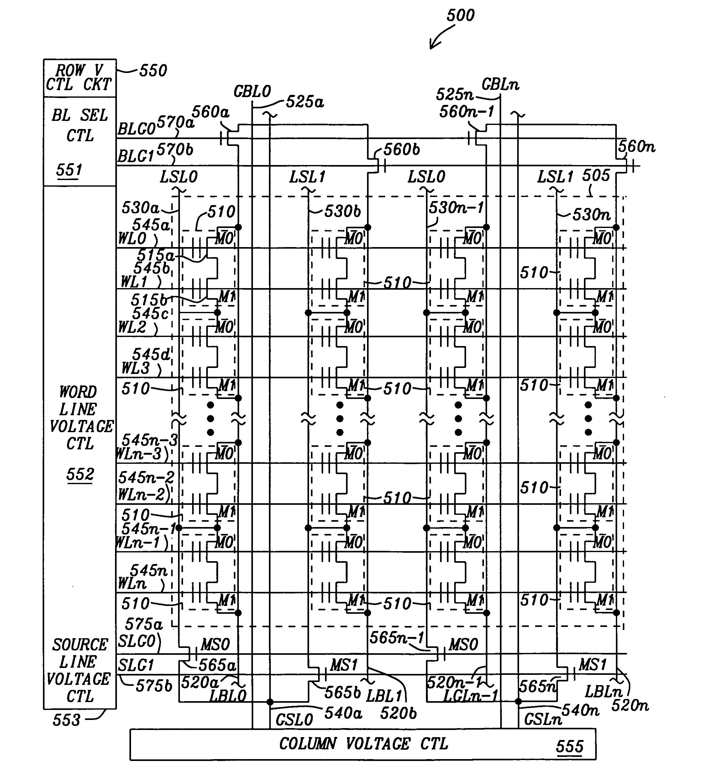
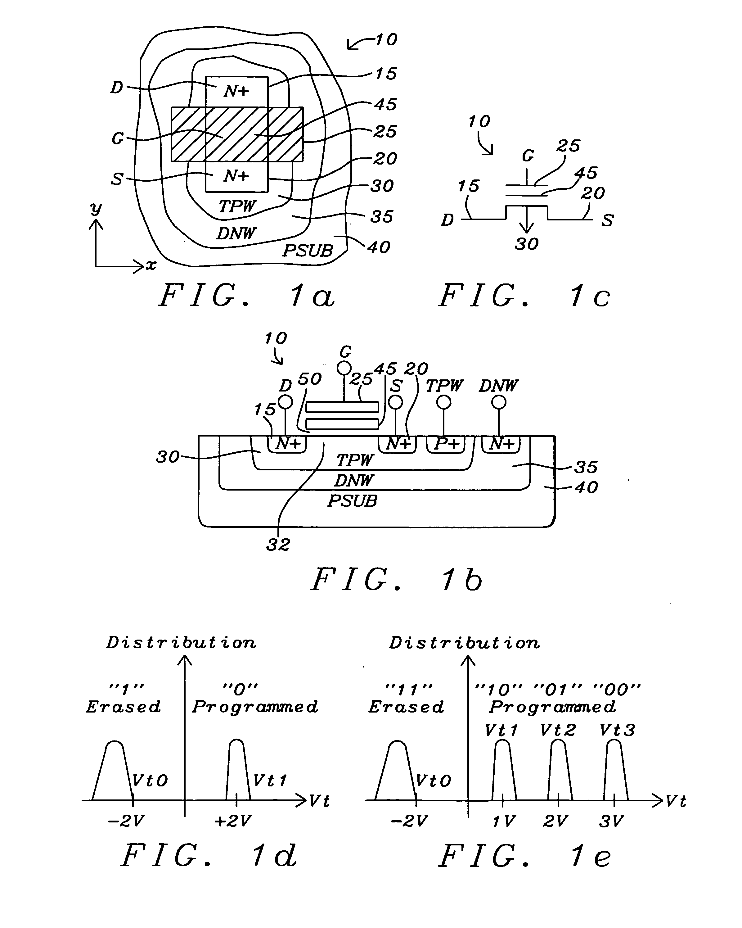
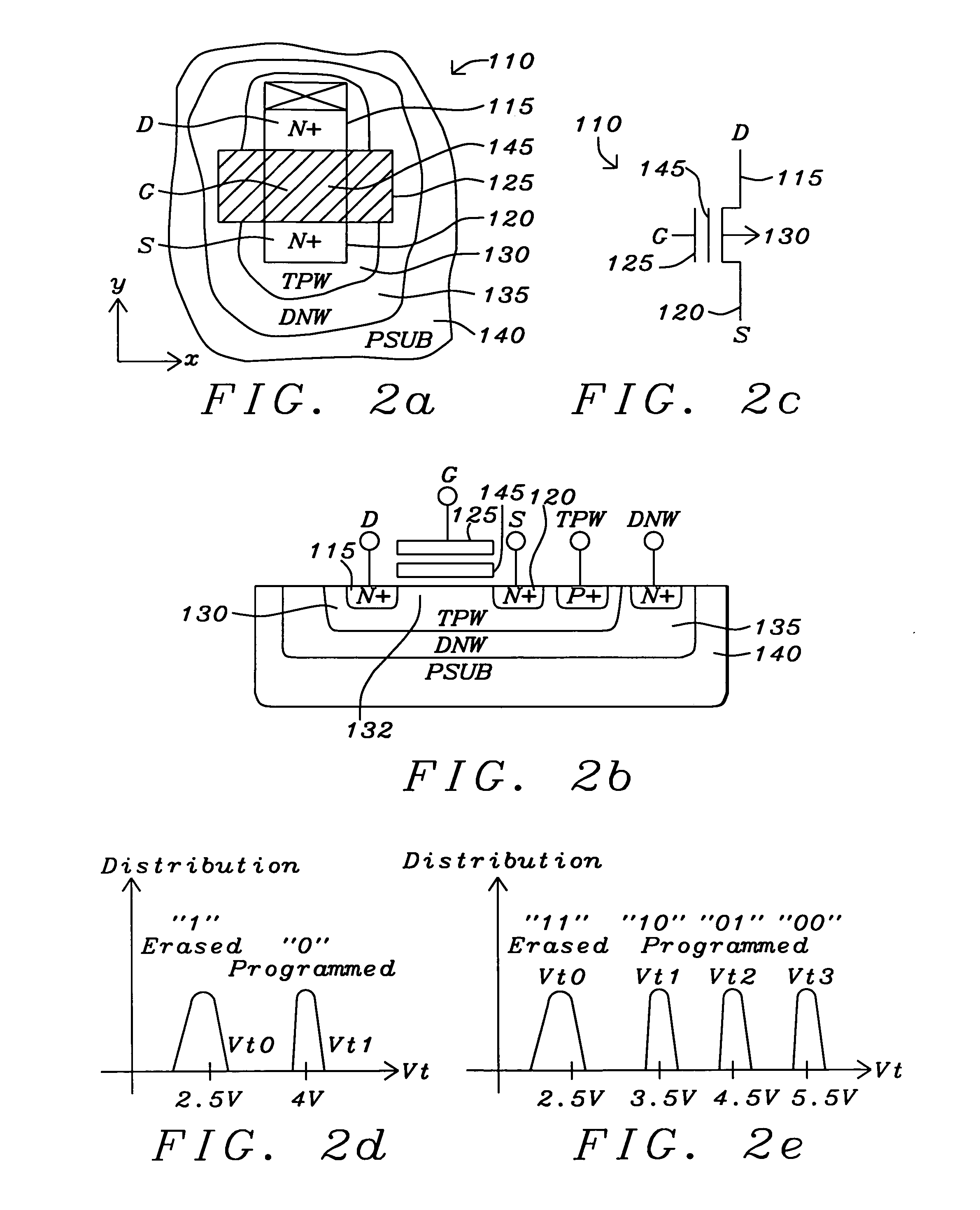
[0077]FIG. 1a is a top plan view of a NMOS NAND flash floating-gate transistor 10. FIG. 1b is a cross sectional view NMOS NAND flash floating-gate transistors 10. FIG. 1c is the schematic symbol NMOS NAND flash floating-gate transistors 10. In a common structure of a NAND cell string of the NMOS NAND flash floating-gate transistors 10, the NMOS NAND flash floating-gate transistors 10 do not require a contact at either the drain diffusion region 15 or source diffusion region 20 node. In conventional NAND cell strings have a top select transistor connected to the topmost transistor and a bottom select transistor connected to the bottommost transistor. The drain of the top select transistor and the source of the bottommost transistor have contacts for connected to bit lines and source lines. This structure for a conventional NAND string enables the size of the NMOS NAND flash floating-gate transistors 10 to be the smallest of the nonvolatile memory structures.

[0078]The floating-gate ty...


PUM

PropertyMeasurementUnit
Electric potential / voltageaaaaaaaaaa

Abstract

A NOR flash nonvolatile memory device provides the memory cell size and a low current program process of a NAND flash nonvolatile memory device and the fast, asynchronous random access of a NOR flash nonvolatile memory device. The NOR flash nonvolatile memory device has an array of NOR flash nonvolatile memory circuits. Each NOR flash nonvolatile memory circuit includes a plurality of charge retaining transistors serially connected in a NAND string. A drain of a topmost charge retaining transistor is connected to a bit line associated with the serially connected charge retaining transistors and a source of a bottommost charge retaining transistor is connected to a source line associated with the charge retaining transistors. Each control gate of the charge retaining transistors on each row is commonly connected to a word line. The charge retaining transistors are programmed and erased with a Fowler-Nordheim tunneling process.

Description

[0001]This application claims priority under 35 U.S.C. §119 to U.S. Provisional Patent Application U.S. Provisional Patent Application Ser. No. 61 / 126,854, filed on May 7, 2008, which is herein incorporated by reference in its entirety.[0002]This application claims priority under 35 U.S.C. §119 to U.S. Provisional Patent Application U.S. Provisional Patent Application Ser. No. 61 / 130,381, filed on May 30, 2008, which is herein incorporated by reference in its entirety.[0003]This application claims priority under 35 U.S.C. §119 to U.S. Provisional Patent Application U.S. Provisional Patent Application Ser. No. 61 / 131,554, filed on Jun. 9, 2008, which is herein incorporated by reference in its entirety.[0004]This application claims priority under 35 U.S.C. §119 to U.S. Provisional Patent Application U.S. Patent Application Ser. No. 61 / 132,122, filed on Jun. 16, 2008, assigned to the same assignee as the present invention, and incorporated herein by reference in its entirety.[0005]This...

Claims


Application Information

Patent Timeline
IPC IPC(8): G11C16/04G11C16/06H01L21/00
CPCG11C11/5628G11C11/5642G11C16/0483G11C16/10Y10T29/41G11C2211/5641H01L27/11519H01L27/11521H01L27/11524G11C16/30H10B41/10H10B41/30H10B41/35
Inventor LEE, PETER WUNGHSU, FU-CHANGTSAO, HSING-YA
Owner APLUS FLASH TECH
Why Eureka
Try Eureka