Imprint apparatus, imprint method, and mold for imprint

a technology of imprinting apparatus and mold, which is applied in the direction of photomechanical equipment, electric/magnetic/electromagnetic heating, instruments, etc., can solve the problems that the gap measurement method disclosed in u.s. pat. no. 6, b2 is not necessarily satisfactory for such a need, and the measurement error is liable to occur, so as to achieve accurate measurement of distan

Inactive Publication Date: 2009-11-19
CANON KK
View PDF24 Cites 11 Cited by
  • Summary
  • Abstract
  • Description
  • Claims
  • Application Information

AI Technical Summary

Benefits of technology

[0018]A specific object of the present invention is to provide an imprint apparatus, an imprint method, and a mold for imprint which are capable of more accurately measuring a distance (gap) between a mold surface and a substrate surface.

Problems solved by technology

However, the gap measurement method disclosed in U.S. Pat. No. 6,696,220 B2 is not necessarily satisfactory for such a need.
However, when these two distances are measured by the method other than that using the interferometer, there arises such a problem that a measurement error is liable to occur.
Accordingly, as described in U.S. Pat. No. 6,696,220 B2, when the optical system for effecting the distance measurement and the optical system for effecting the in-plane position measurement are separately provided, it is difficult to dispose these optical systems together in the same area.
For this reason, there is a problem such that it is difficult to prevent an error in distance measurement caused by positional deviation between the mold and the substrate due to a temperature change, vibration, etc.

Method used


Image

  • Imprint apparatus, imprint method, and mold for imprint
  • Imprint apparatus, imprint method, and mold for imprint
  • Imprint apparatus, imprint method, and mold for imprint

Examples


embodiment 1

[0051]In Embodiment 1, a constitutional example of an imprint apparatus according to the present invention will be described.

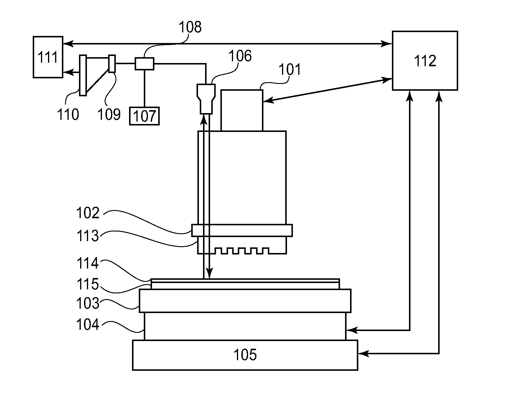
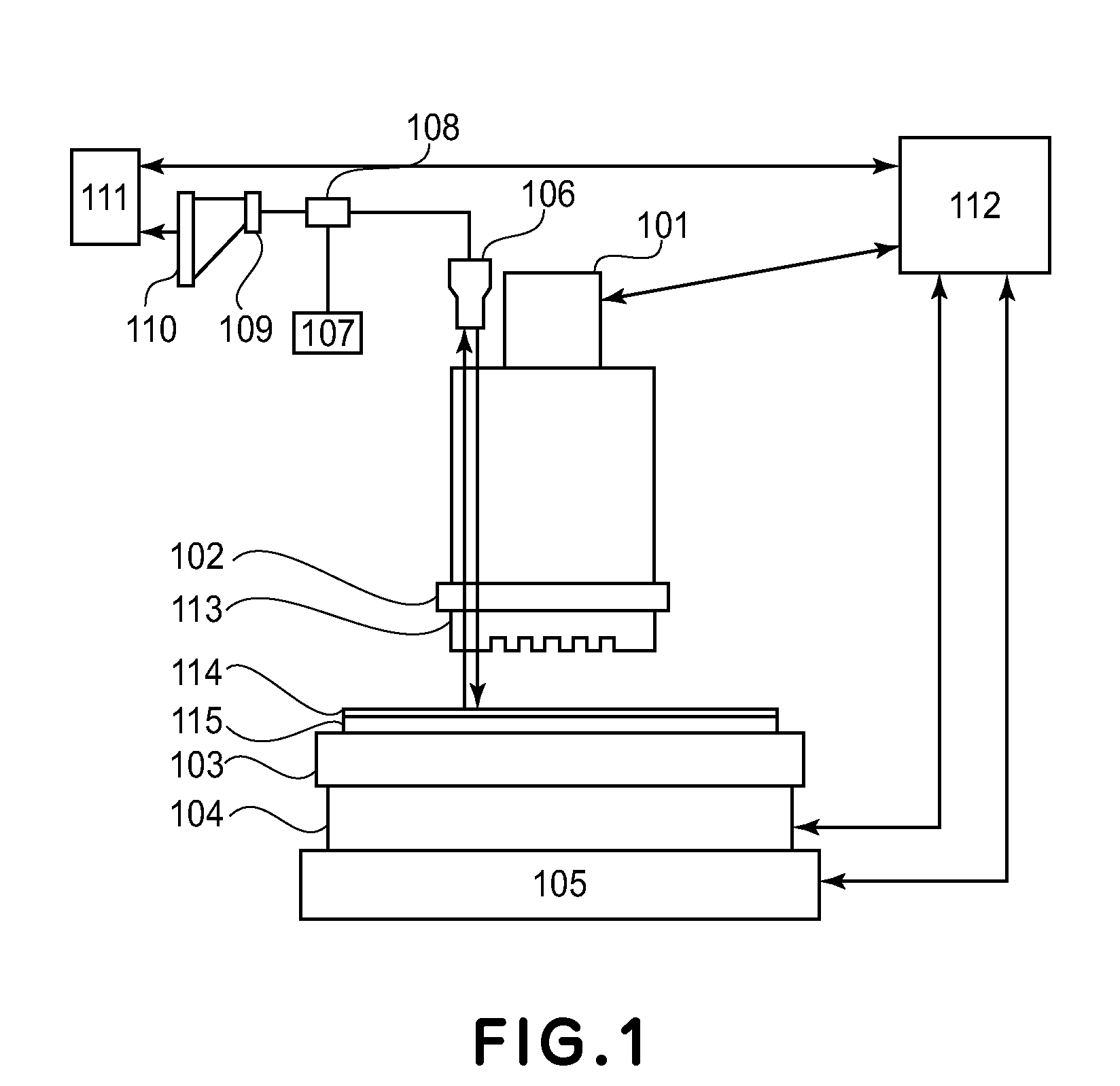
[0052]FIG. 1 shows the constitutional example of the imprint apparatus in Embodiment 1.

[0053]Referring to FIG. 1, the imprint apparatus includes an exposure light source 101, a mold holding portion 102, a work holding portion 103, a work pressing mechanism 104, an in-plane moving mechanism 105, an optical system 106, a measurement light source 107, a beam splitter 108, a spectroscope 109, an image-pickup device 110, an analyzer 111, an imprint control mechanism 112, a mold 113, a photo-curable resin material 114, and a substrate 115.

[0054]The mold holding portion 102 effects chucking of the mold 113 by a vacuum chuck method or the like. A work or workpiece is movable to a desired position by the in-plane moving mechanism 105. The work pressing mechanism 104 is capable of adjusting a height of the work and applying pressure to the work.

[0055]Incidentally, a pos...

embodiment 2

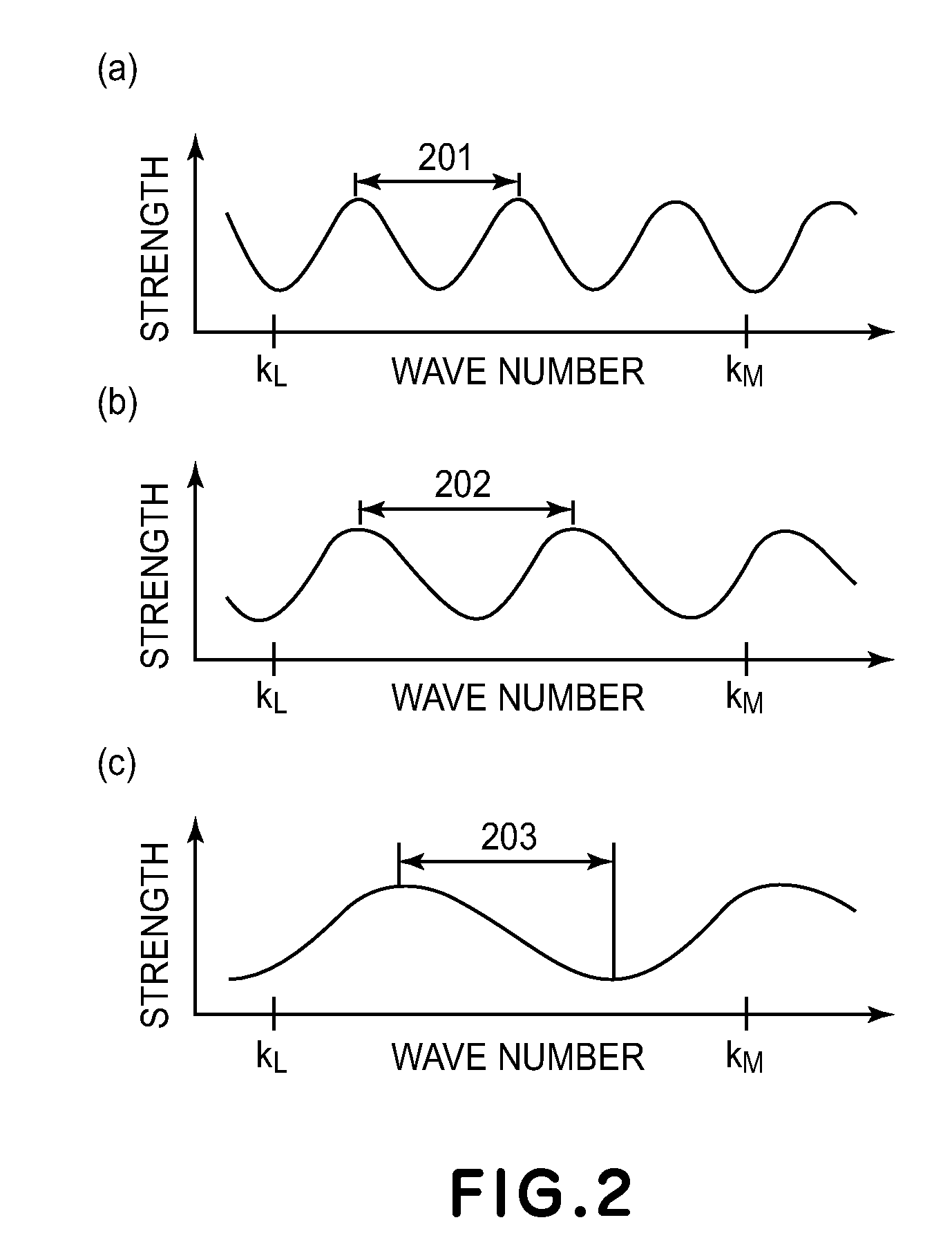
[0108]In Embodiment 2, a mold using a boundary surface between two members as the measurement surface and a measuring method using the mold will be described. This embodiment is useful in that it is applicable to even the case where the coherence length is shorter than the mold thickness.

[0109]FIG. 5(a) shows a mold constitution using, as the measurement surface, the boundary surface between two members. This mold is constituted by a first member 401 and a second mold 407. The boundary surface between these first and second member 401 and 407 is indicated by a reference numeral 408. Further, the first member 401, the second member 407, and a photocurable resin material are constituted by materials different in refractive index.

[0110]As a material for the second member 407, it is possible to use titanium oxide (n: nearly equal to 2.4), ITO (n: nearly equal to 2), silicon nitride (n: nearly equal to 2), etc. Further, the thickness of the second member 407 may desirably be ¼ or more of...

embodiment 3

[0118]In Embodiment 1, the mold thickness is measured by utilizing the mold back surface as the measurement surface, in the case where the coherence length of broadband light is longer than the mold thickness, to calculate the distance between the mold surface and the substrate surface.

[0119]Further, in Embodiment 2, the distance between the mold surface and the substrate surface can be calculated by using the boundary surface between the two members as the measurement surface even in the case where the coherence length of broadband light is shorter than the mold thickness.

[0120]In these embodiments, however, in the case where the coherence length of broadband light is shorter than the mold thickness and the second member cannot be provided to the mold, there is such a problem that the distance between the mold surface and the substrate surface cannot be measured.

[0121]In Embodiment 3, a measuring method that solves such a problem will be described.

[0122]FIG. 7(a) is a schematic vie...


PUM

PropertyMeasurementUnit
diameteraaaaaaaaaa
diameteraaaaaaaaaa
refractive indexaaaaaaaaaa

Abstract

An imprint apparatus for imprinting a mold pattern onto a substrate or a member on the substrate includes a light source for irradiating a surface of the mold disposed opposite to the substrate and a surface of the substrate with light; an optical system for guiding the light from the light source to the surface of the mold and the surface of the substrate and guiding reflected lights from these surfaces to a spectroscope; a spectroscope for dispersing the reflected lights guided by the optical system into a spectrum; and an analyzer for analyzing a distance between the surface of the mold and the surface of the substrate. The analyzer calculates the distance between the surface of the mold and the surface of the substrate by measuring a distance between the surface of the mold and a surface formed at a position away from the surface of the mold.

Description

CROSS-REFERENCE TO RELATED APPLICATIONS[0001]This application is a division of application Ser. No. 11 / 719,434, which is the National Stage of International Application No. PCT / JP2006 / 321187, filed Oct. 18, 2006, and which is incorporated herein by reference.TECHNICAL FIELD[0002]The present invention relates to an imprint apparatus and imprint method, which are used for imprinting a pattern provided to a mold onto a substrate or a member on the substrate and also relates to a mold for imprint.BACKGROUND ART[0003]In recent years, as proposed in Appl. Phys. Lett., Vol. 67, Issue 21, pp. 3114-3116 (1995) by Stephan Y. Chou et al., a technology for transferring a fine pattern provided on a mold onto a semiconductor, glass, resin, metal or the like has been developed and has received attention. This technology is called nanoimprint or nanoembossing since it has resolving power on the order of several nanometers. By utilizing this technology, it is possible to process a three-dimensional ...

Claims


Application Information

Patent Timeline
Patent Type & Authority Applications(United States)
IPC IPC(8): B29C59/16B29C35/08
CPCB82Y10/00B82Y40/00G03F7/0002B29C59/16G03F9/7042G03F9/7065B29C35/08G03F9/703G01B11/14
Inventor SUEHIRA, NOBUHITOSEKI, JUNICHIINA, HIDEKI
Owner CANON KK
Why Eureka
Try Eureka