Organic el display panel and manufacturing method thereof

Active Publication Date: 2009-11-19
JOLED INC
View PDF17 Cites 64 Cited by
  • Summary
  • Abstract
  • Description
  • Claims
  • Application Information

AI Technical Summary

Benefits of technology

[0016]A polymer organic EL display panel of the present invention includes functional layers (e.g., polymer organic EL layer) having uniform thickness held between the cathode electrode and anode electrode and thus shows improved light-emitting characteristics over conventional display panels. In addition,

Problems solved by technology

However, with the second method, the thickness of an o

Method used


Image

  • Organic el display panel and manufacturing method thereof
  • Organic el display panel and manufacturing method thereof
  • Organic el display panel and manufacturing method thereof

Examples


Example

Embodiment 1

[0142]In Embodiment 1, an active matrix type organic EL display panel in which a hole transport layer is provided as a single layer by means of plane formation will be described.

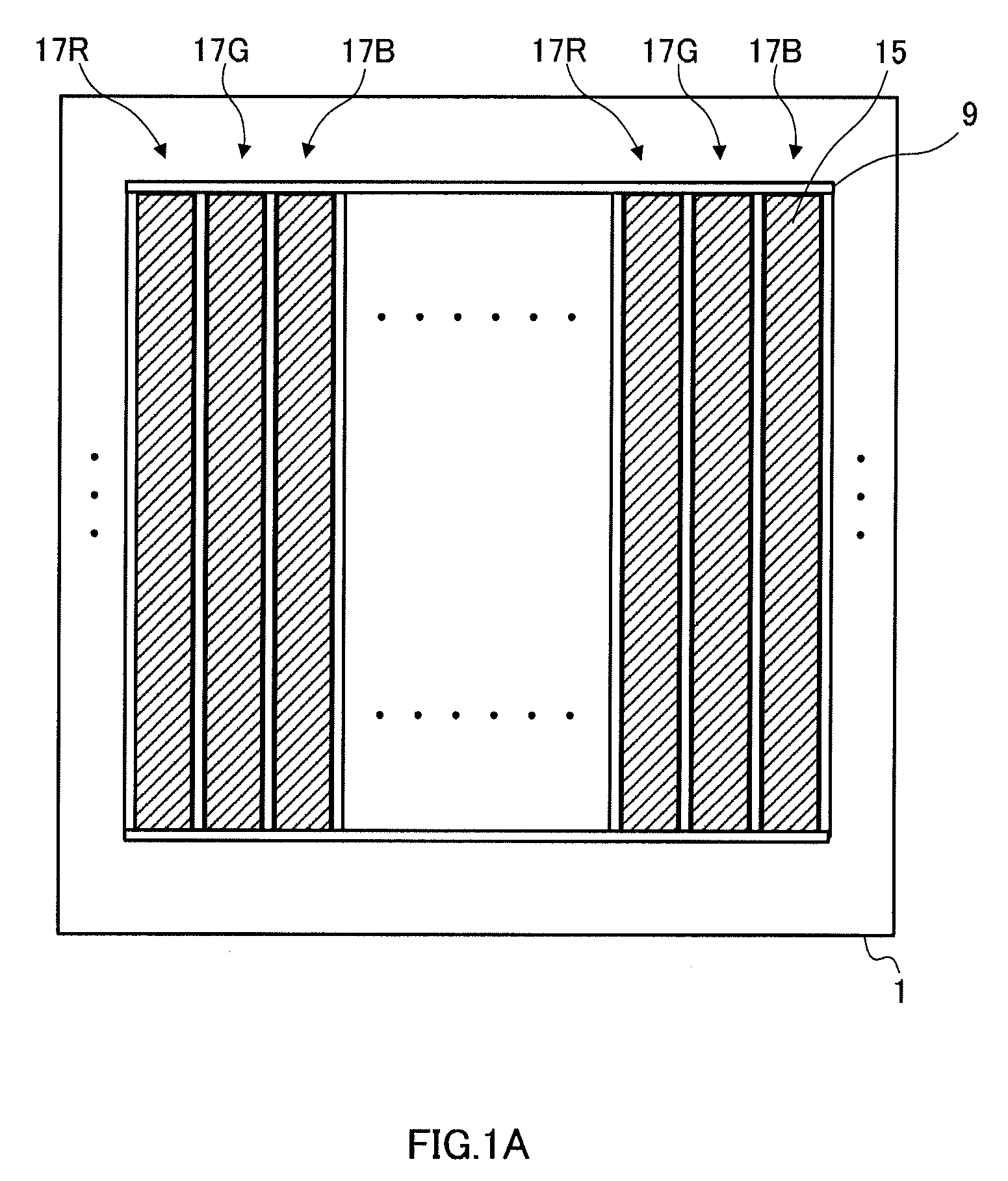
[0143]FIG. 1A is a plan view of an active matrix type organic EL display panel. In the panel shown in FIG. 1A, line-state first banks 9 formed are provided. First banks 9 define pixel regions 17. The pixel regions 17 are of three types: pixel regions 17R emitting red light; pixel regions 17G emitting green light; and pixel regions 17B emitting blue light. These three types of pixel regions are arranged in order. Pixel regions 17 are covered by cathode electrode 15 and separated by first banks 9 as discrete pixel regions.

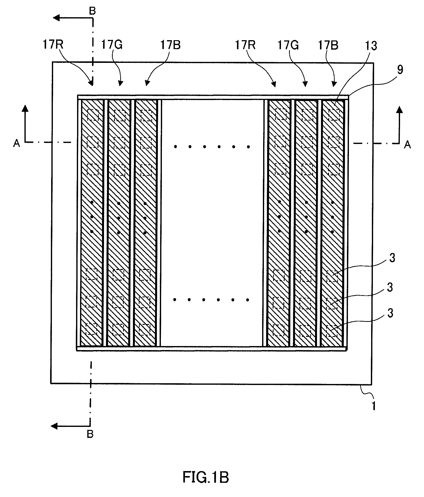
[0144]FIG. 1B is a plan view of the organic EL display panel of active matrix type of the present embodiment from which the cathode electrode is removed.

[0145]FIG. 2A shows a line A-A sectional view of the organic EL display panel of the present embodiment shown in FIG. 1B. FIG. 2...

Example

Embodiment 2

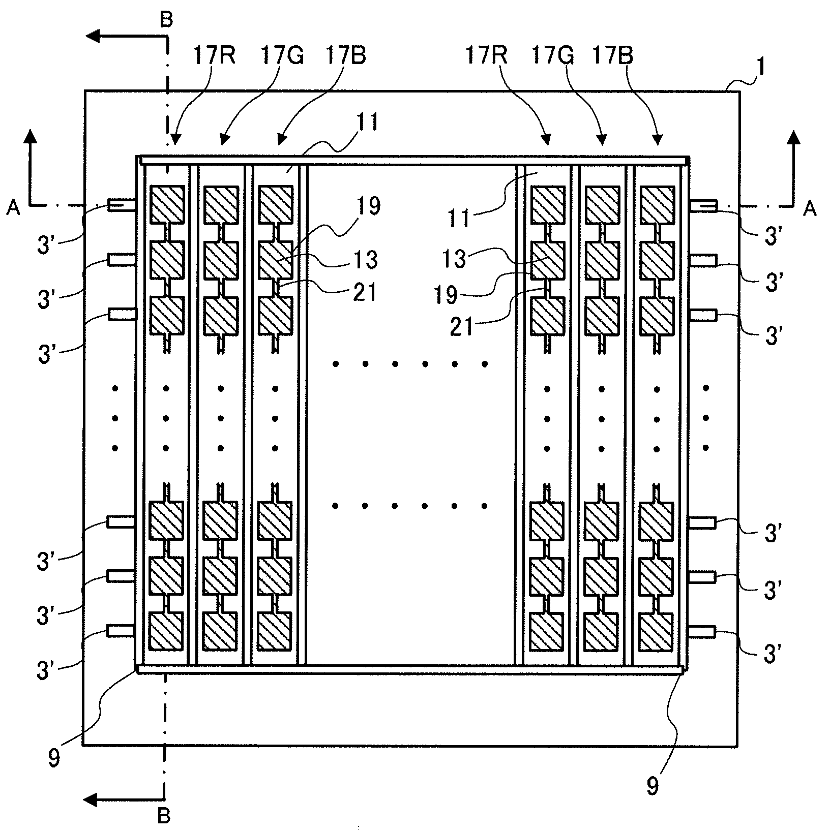
[0147]In Embodiment 1, the active matrix type organic EL display panel was explained. In Embodiment 2, a passive matrix type organic EL display panel will be described. In the present embodiment, the organic EL display panel has second banks.

[0148]FIG. 3 is a plan view of a state where cathode electrode 15 is removed from the organic EL display in the present embodiment. In the panel shown in FIG. 3, substrate 1, line-state anode electrodes 3′, and line-state first banks 9 are set. The line direction (lateral direction in the figure) of anode electrodes 3′, and the line direction (vertical direction in the figure) of first banks 9 are orthogonal to each other.

[0149]Inside pixel region 17, two or more sub pixel regions 19 defined by second banks 11 are set. Adjacent sub pixel regions 19 in region 17 are connected with each other by grooves 21. In sub pixel regions 19 and grooves 21, polymer organic EL material 13 with corresponding color is provided.

[0150]FIG. 4A shows a ...

Example

Embodiment 3

[0156]In Embodiments 1 and 2, the organic EL display panel in which the hole transport layer is formed as a single layer by means of plane formation and the interlayer is formed in lines was described. For Embodiment 3, the organic EL display panel in which the interlayer is formed as a single layer by means of plane formation will be described. The organic EL display panel of the present embodiment is the passive matrix type and has second banks.

[0157]The plan view of the organic EL display panel of the present embodiment is the same as that of Embodiment 2. Therefore, FIG. 3 is also a plan view of the organic EL display panel of the present embodiment.

[0158]FIG. 5A shows a line A-A sectional view of the organic EL display panel of the present embodiment shown in FIG. 3. FIG. 5B shows a line B-B sectional view of the organic EL display panel of the present embodiment shown in FIG. 3.

[0159]As shown in FIGS. 5A and 5B, the organic EL display panel of the present embodimen...


PUM

PropertyMeasurementUnit
Transport propertiesaaaaaaaaaa

Abstract

An organic EL display panel having a polymer organic EL layer with a uniform thickness is provided. The organic EL display panel includes a substrate, anode electrodes set on the substrate; a hole transport layer provided on the substrate on which the anode electrodes are set; banks provided in lines on the hole transport layer to define line-state pixel regions; an interlayer set in a line in the pixel region; a polymer organic EL layer set in a line on the interlayer in the pixel region; and a cathode electrode provided on the polymer organic EL layer.

Description

TECHNICAL FIELD[0001]The present invention relates to an organic EL (OEL) display panel and a manufacturing method thereof.BACKGROUND ART[0002]An OEL display panel is a display panel that uses light-emitting elements exploiting electro-luminescence of organic compounds. That is, the OEL display panel has a cathode, an anode, and organic compound-containing EL elements for electro-luminescense which are provided between the electrodes. Electro-luminescent organic compounds can be roughly classified into combinations of low-molecular organic compounds (host material and dopant material) and high-molecular organic compounds (polymer organic compounds). Examples of the electro-luminescent polymer organic compounds include polyphenylenevinylene (also referred to as PPV) and its derivatives. The OEL display panel using the electro-luminescent polymer organic compound is driven with a relatively low voltage, consumes less power and is considered to be capable of contributing to display pan...

Claims


Application Information

Patent Timeline
IPC IPC(8): H01J1/63
CPCH01L27/3211H01L27/3246H05B33/22H01L51/5048H01L27/3283H10K59/35H10K59/122H10K59/173H10K50/14H01L2924/01042H10K59/12H10K50/15
Inventor YOSHIDA, HIDEHIROKITAMURA, YOSHIROYAMAMURO, KEISEI
Owner JOLED INC
Why Eureka
Try Eureka