Method and apparatus for pulsed plasma processing using a time resolved tuning scheme for RF power delivery

a pulsed plasma and power delivery technology, applied in the direction of electric variable regulation, process and machine control, instruments, etc., can solve the problems of arcing within dielectric layers, destructive currents, and uneven charge accumulation across wafers

Active Publication Date: 2009-11-19
APPLIED MATERIALS INC
View PDF9 Cites 425 Cited by
  • Summary
  • Abstract
  • Description
  • Claims
  • Application Information

AI Technical Summary

Benefits of technology

[0014]In some embodiments, a method for tuning a system operating a plasma process in a time resolved manner using a source RF power supply and a bias RF power supply, each capable of frequency tuning and respectively coupled to a process chamber via a source matching network and a bias matching network may be provided. The method may include igniting a plasma in a process chamber using the source RF power supply and the bias RF power supply, each independently set in a first operational mode selected from either a continuous wave mode or a pulsing mode and in a first tuning mode selected from either a fixed frequency mode or a frequency tuning mode, with the source matching network and the bias matching network each in...

Problems solved by technology

This charge accumulation may not be uniform across the wafer.
As such the charge accumulation may cause destructive currents to be induced in some of the metalized materials and/or cause arcing within dielectric layers.
The currents and/or arcing may destroy or damage certain devices that have previously been formed on the wafer.
One drawback of using a pulsed plasma etch reactor is that the power from an RF generator or RF source must be coupled through a dynamically tuned matching network (also referred to as a match unit) to an antenna or electrode within a plasma reactor.
Since the matching networks ...

Method used


Image

  • Method and apparatus for pulsed plasma processing using a time resolved tuning scheme for RF power delivery
  • Method and apparatus for pulsed plasma processing using a time resolved tuning scheme for RF power delivery
  • Method and apparatus for pulsed plasma processing using a time resolved tuning scheme for RF power delivery

Examples


Embodiment Construction

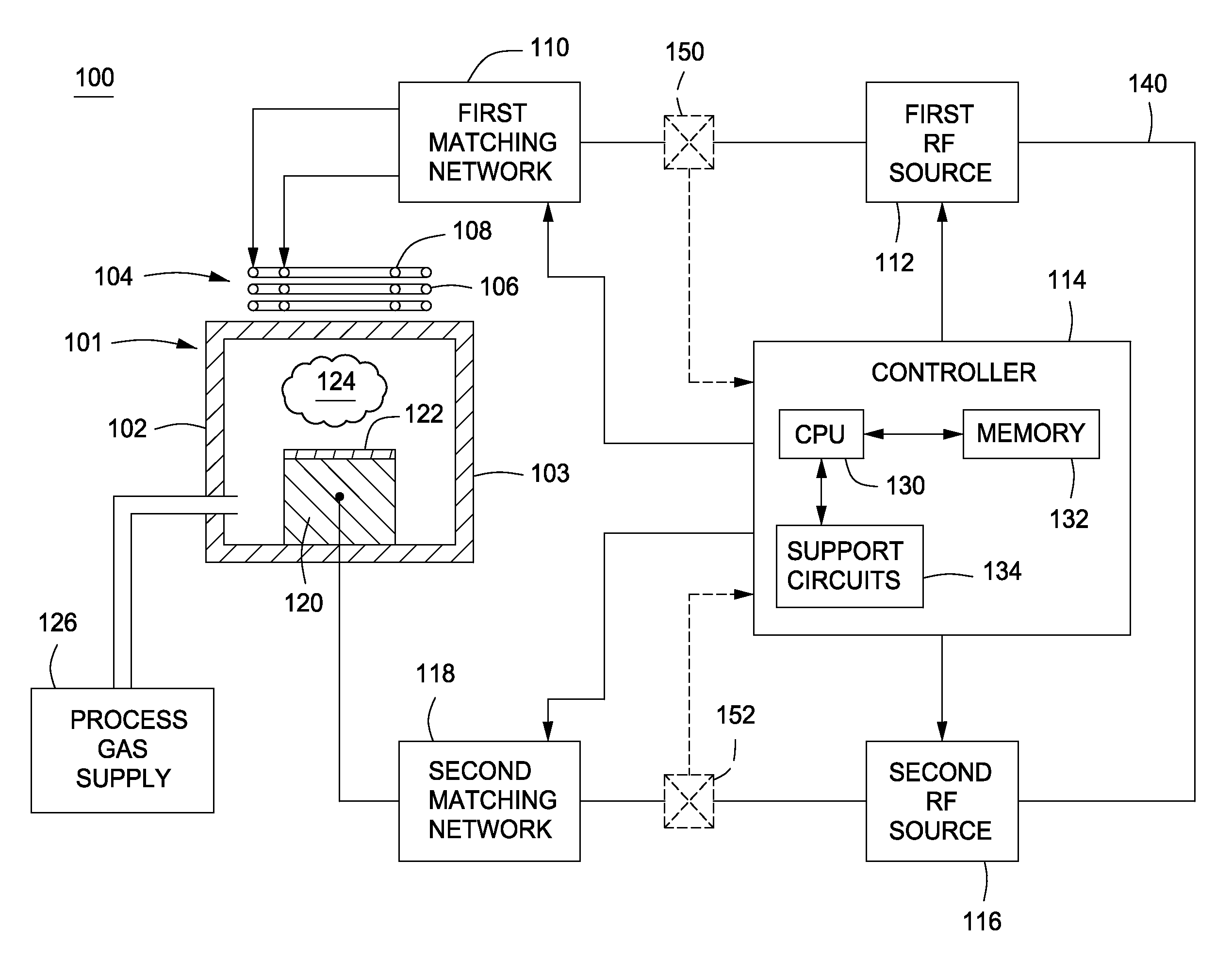
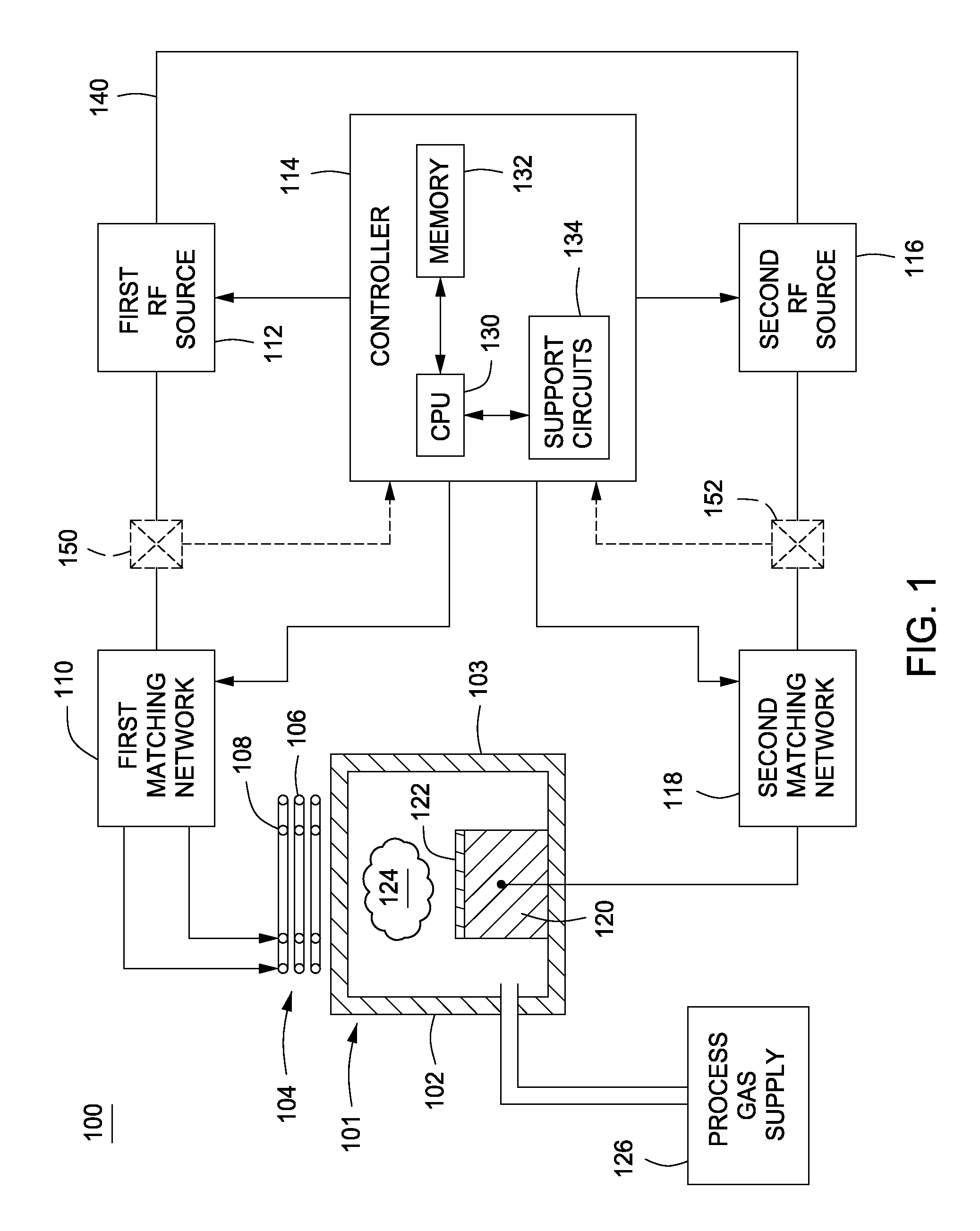
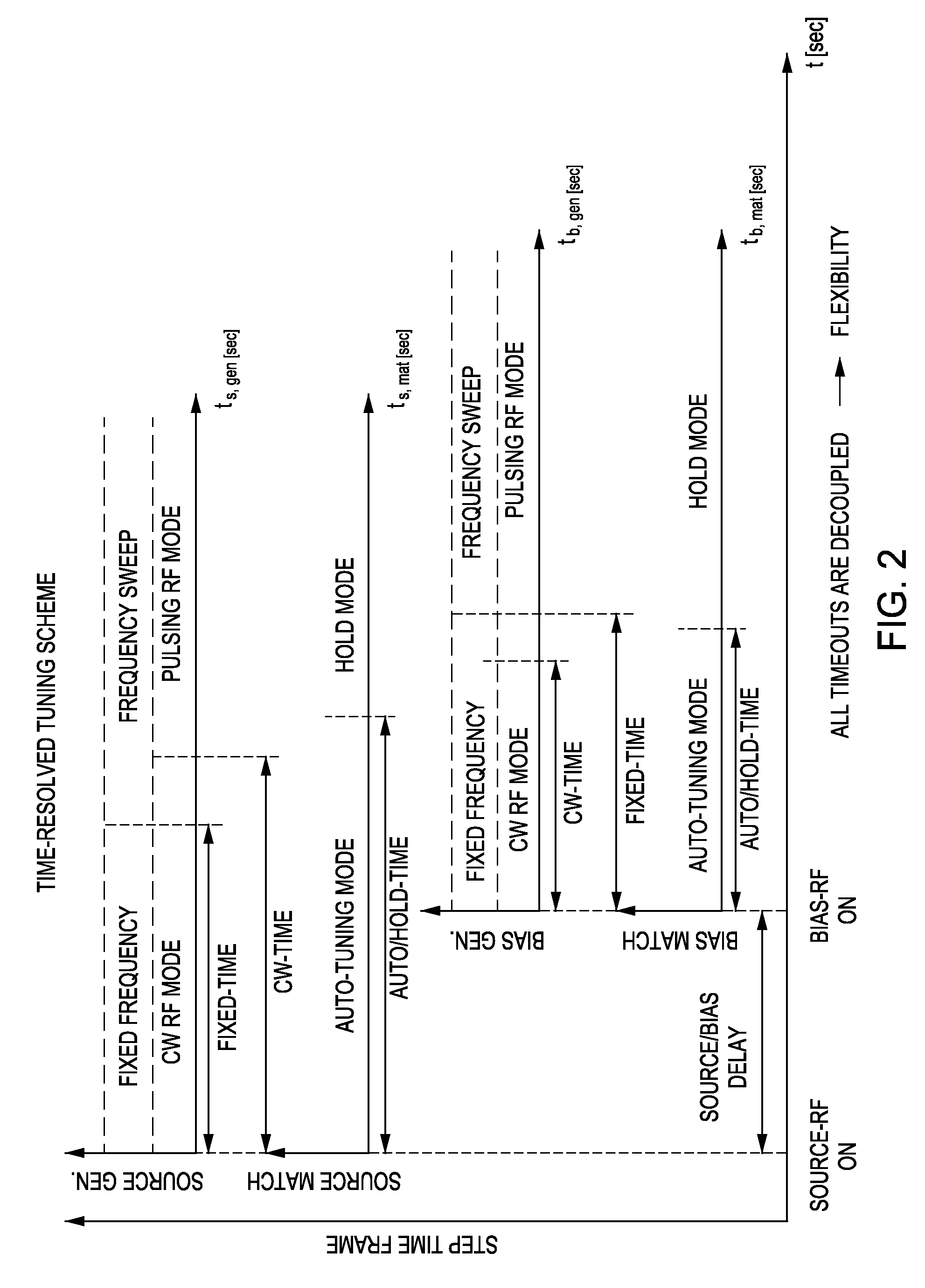
[0021]The present invention provides methods and apparatus for processing substrates using a pulsed plasma. In some embodiments, a plasma pulsing process for either or both of the bias and the source that may facilitate better performance (better etch uniformity and selectivity) with less damage at the wafer level as well as reducing trenching and notching problems. Embodiments of the present invention provides procedures that enable a stable window of operation for pulsing mode using the RF generators having frequency tuning (also referred to as frequency sweep) in combination with dynamic matching networks. As the time needed to get the system tuned is critical during the etch process, one advantage of these procedures is being able to tune within less than about 6 sec while pulsing, thereby minimizing the time during which the wafer is exposed to unstable plasma. Although the description below may refer to certain processes, RF frequencies, and RF powers, the teachings provided h...


PUM


Abstract

Embodiments of the present invention generally provide methods and apparatus for pulsed plasma processing over a wide process window. In some embodiments, an apparatus may include an RF power supply having frequency tuning and a matching network coupled to the RF power supply that share a common sensor for reading reflected RF power reflected back to the RF power supply. In some embodiments, an apparatus may include an RF power supply having frequency tuning and a matching network coupled to the RF power supply that share a common sensor for reading reflected RF power reflected back to the RF power supply and a common controller for tuning each of the RF power supply and the matching network.

Description

CROSS REFERENCE TO RELATED APPLICATIONS[0001]This application claims the benefit of U.S. Provisional Patent Application Ser. No. 61 / 127,634, filed May 14, 2008, which is herein incorporated by reference.BACKGROUND[0002]1. Field[0003]Embodiments of the present invention generally relate to semiconductor substrate processing systems and, more specifically, to methods and apparatus for processing substrates using a pulsed plasma.[0004]2. Description of the Related Art[0005]In semiconductor integrated circuit (IC) fabrication, devices such as component transistors are formed on a semiconductor wafer substrate that is typically made of silicon. During the fabrication process, various materials are deposited on different layers in order to build or form the desired integrated circuit. The various layers define devices that are interconnected by metallization lines. During certain plasma enhanced processes that are performed upon wafers (also referred to in the art as substrates) that alre...

Claims


Application Information

Patent Timeline
IPC IPC(8): H05B31/26
CPCH01J37/32155H01J37/32174H01J37/32146H01J37/321H01L21/3065H05H1/46
Inventor BANNA, SAMERTODOROW, VALENTINRAMASWAMY, KARTIK
Owner APPLIED MATERIALS INC
Why Eureka
Try Eureka