Method and System for Forming Patterns with Charged Particle Beam Lithography

Active Publication Date: 2012-12-27
D2S
View PDF0 Cites 49 Cited by
  • Summary
  • Abstract
  • Description
  • Claims
  • Application Information

AI Technical Summary

Benefits of technology

[0016]A method for fracturing or mask data preparation or mask process correction for charged particle beam lithography is disclosed in which a plurality of shots are determined that will form a pattern on a surface, where shots are determined so as to reduce sensitivity of the resulting pattern to changes in βf. At least some shots in the plurality of shots overlap other shots. In some embodiments, βf is reduced

Problems solved by technology

An example of an end-use limitation is defining the geometry of a transistor in a way in which it cannot sufficiently operate at the required supply voltage.
The design rule limitations reflect, among other things, the smallest dimensions that can be reliably fabricated.
As the critical dimensions of the circuit pattern become smaller and approach the resolution value of the exposure tool, the accurate transcription of the physical design to the actual circuit pattern developed on the resist layer becomes difficult.
Adding OPC features is a very laborious task, requires costly computation time, and results in more expensive reticles.
Not only are OPC patterns complex, but since optical proximity effects are long range compared to minimum line and space dimensions, the correct OPC patterns in a given location depend significantly on what other geometry is in the neighborhood.

Method used


Image

  • Method and System for Forming Patterns with Charged Particle Beam Lithography
  • Method and System for Forming Patterns with Charged Particle Beam Lithography
  • Method and System for Forming Patterns with Charged Particle Beam Lithography

Examples


Embodiment Construction

[0036]The improvements and advantages of the present disclosure can be accomplished by controlling the parameters of the shots forming a pattern, so as to reduce the magnitude of pattern variations caused by variation of βf, thereby allowing higher quality patterns to be formed on reticles and other surfaces such as wafers.

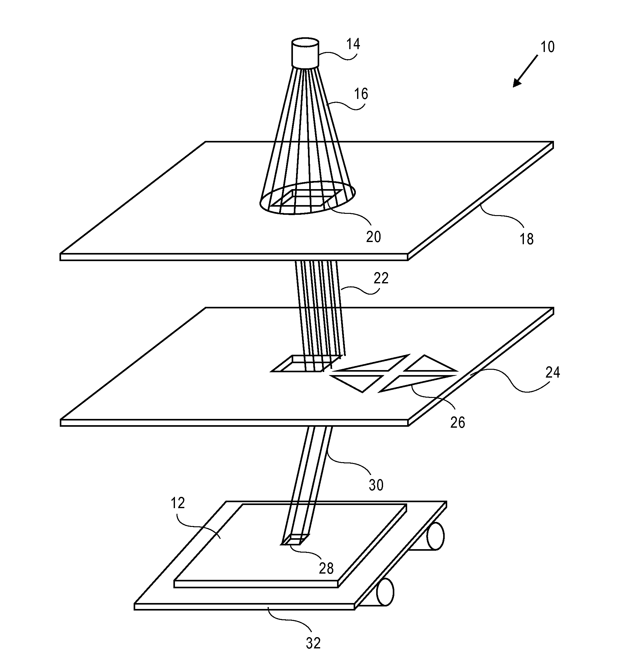
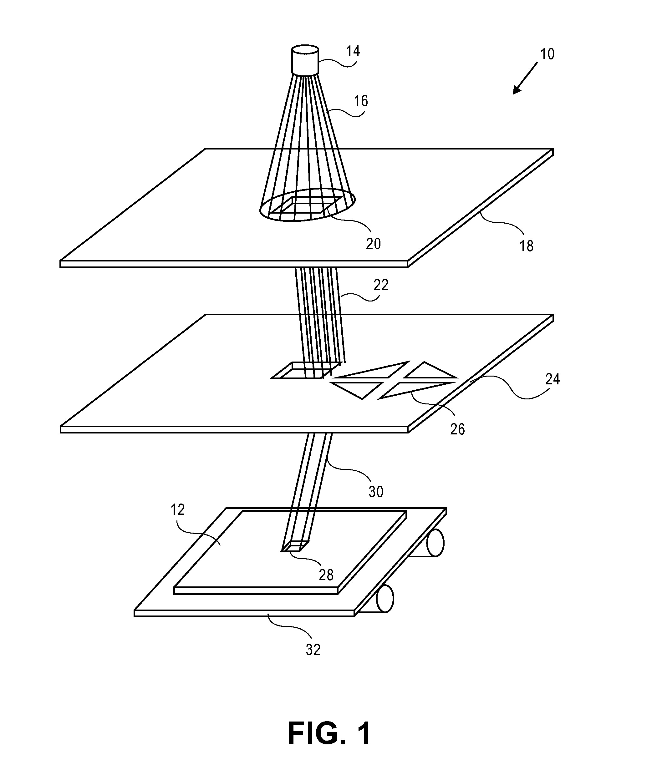
[0037]Referring now to the drawings, wherein like numbers refer to like items, FIG. 1 identifies an embodiment of a lithography system, such as a charged particle beam writer system, in this case an electron beam writer system 10, that employs a variable shaped beam (VSB) to manufacture a surface 12 according to the present disclosure. The electron beam writer system 10 has an electron beam source 14 that projects an electron beam 16 toward an aperture plate 18. The plate 18 has an aperture 20 formed therein which allows the electron beam 16 to pass. Once the electron beam 16 passes through the aperture 20 it is directed or deflected by a system of lenses (not sho...


PUM


Abstract

In a method for fracturing or mask data preparation or mask process correction for charged particle beam lithography, a plurality of shots are determined that will form a pattern on a surface, where shots are determined so as to reduce sensitivity of the resulting pattern to changes in beam blur (βf). At least some shots in the plurality of shots overlap other shots. In some embodiments, βf is reduced by controlling the amount of shot overlap in the plurality of shots, either during initial shot determination, or in a post-processing step. The reduced sensitivity to βf expands the process window for the charged particle beam lithography process.

Description

RELATED APPLICATIONS[0001]This application is related to Fujimura, U.S. patent application Ser. No. ______, entitled “Method and System for Forming High Accuracy Patterns Using Charged Particle Beam Lithography” (Attorney Docket No. D2SiP035) filed on even date herewith; which is hereby incorporated by reference for all purposes.BACKGROUND OF THE DISCLOSURE[0002]The present disclosure is related to lithography, and more particularly to the design and manufacture of a surface which may be a reticle, a wafer, or any other surface, using charged particle beam lithography.[0003]In the production or manufacturing of semiconductor devices, such as integrated circuits, optical lithography may be used to fabricate the semiconductor devices. Optical lithography is a printing process in which a lithographic mask or photomask manufactured from a reticle is used to transfer patterns to a substrate such as a semiconductor or silicon wafer to create the integrated circuit (I.C.). Other substrates...

Claims


Application Information

Patent Timeline
IPC IPC(8): H01L21/26G06F17/50G21K5/00
CPCH01J37/3174H01J2237/31764H01J2237/31771H01J2237/31776G03F1/78B82Y40/00G03F1/20G03F7/2037H01L21/027Y10S430/143B82Y10/00G03F7/2063
Inventor FUJIMURA, AKIRABORK, INGO
Owner D2S
Why Eureka
Try Eureka