Multilayer hardmask scheme for damage-free dual damascene processing of SiCOH dielectrics

a dielectric and damage-free technology, applied in the field of integrated circuits, can solve the problems of increasing the number of integrated circuits, ash-induced modification, and affecting the efficiency of the routing of these signals across the device, so as to facilitate the creation of the dual damascene structure, improve performance, reliability, and function

Active Publication Date: 2006-07-13
GLOBALFOUNDRIES US INC
View PDF7 Cites 47 Cited by
  • Summary
  • Abstract
  • Description
  • Claims
  • Application Information

AI Technical Summary

Benefits of technology

[0011] An even further object of the present invention is to provide an interconnect structure in which there is negligible ILD modification, even for ULK SiCOH dielectrics.
[0012] A still further object of the present invention is to provide an interconnect structure formed by a dual damascene process that has a large dual damascene etch process window. A large process window facilitates creation of the dual damascene structure irrespective of variations in film thickness and etch rate variations due to tool condition, in addition to across wafer, wafer-to-wafer, lot-to-lot, and tool-to-tool variations.
[0013] Another object of the present invention is to provide an interconnect structure that has improved performance, reliability, and functionality.

Problems solved by technology

Efficient routing of these signals across the device can become more difficult as the complexity and number of integrated circuits are increased.
For given integration strategies, one of the major challenges associated with the fabrication of thin and fatwires for 90 nm and beyond CMOS BEOL technologies is the issue of ash induced modification of the organosilicate glass (OSG) based ILD materials during damascene processing.
However, there are at least 3 problems with the prior art technique disclosed in the '096 patent.
First, the etch resistance of the metallic nitride layer 24 is typically insufficient for providing substantial process window in a manufacturing environment.
Though one can achieve an excess of 1:1 selectivity for the hardmask layers and SiCOH-based ILD relative to the metallic nitride layer 24, to enable lithography the metallic nitride layer 24 disclosed in the '096 patent must be thin (on the order of about 35 nm or less) and retention of this relatively thin layer is challenging and is nearly impossible.
Second, the metal nitride layer 24 is costly to deposit.
The prior art technique disclosed in the '096 patent avoids ILD damage, but is costly, requires dedicated etch tools, and does not provide a large dual damascene process window.

Method used


Image

  • Multilayer hardmask scheme for damage-free dual damascene processing of SiCOH dielectrics
  • Multilayer hardmask scheme for damage-free dual damascene processing of SiCOH dielectrics
  • Multilayer hardmask scheme for damage-free dual damascene processing of SiCOH dielectrics

Examples


Embodiment Construction

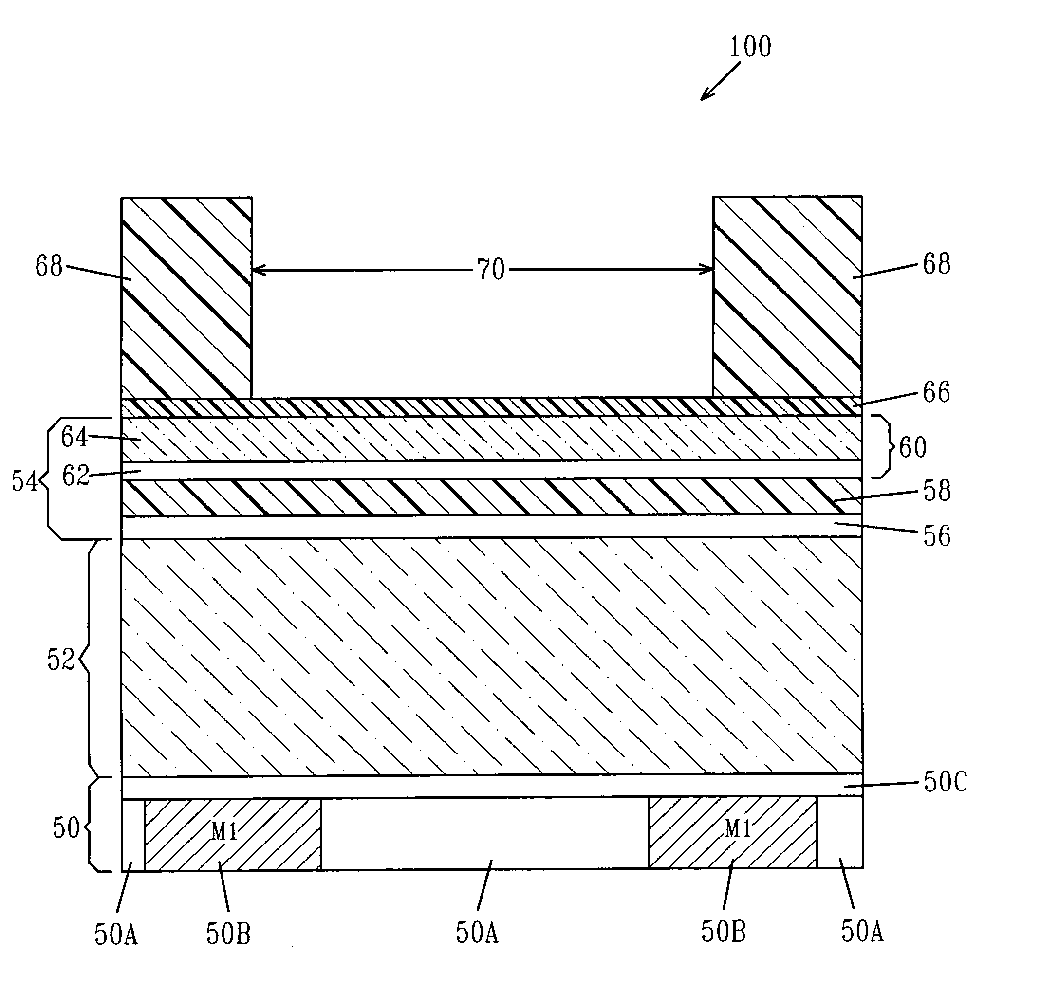
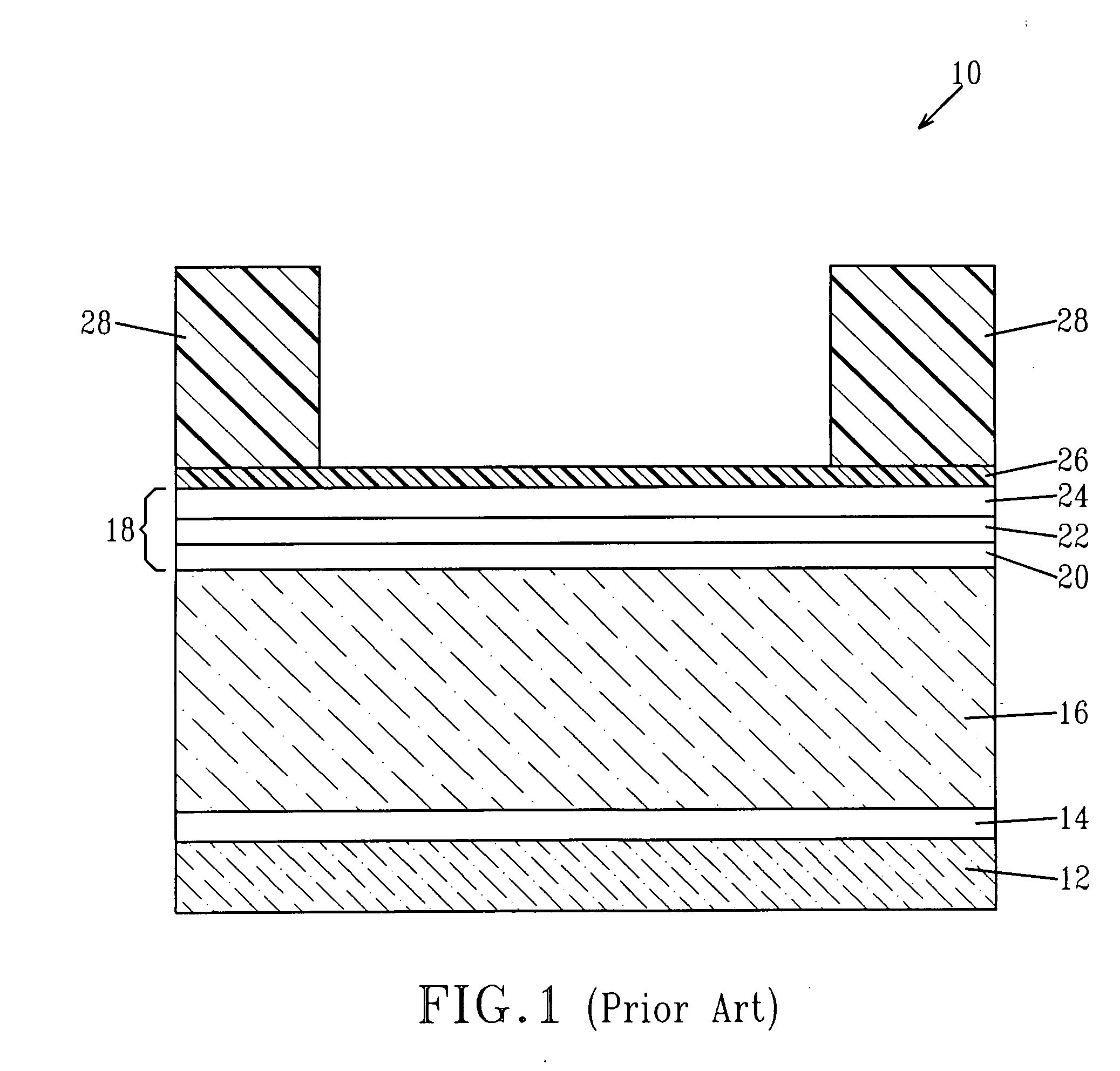
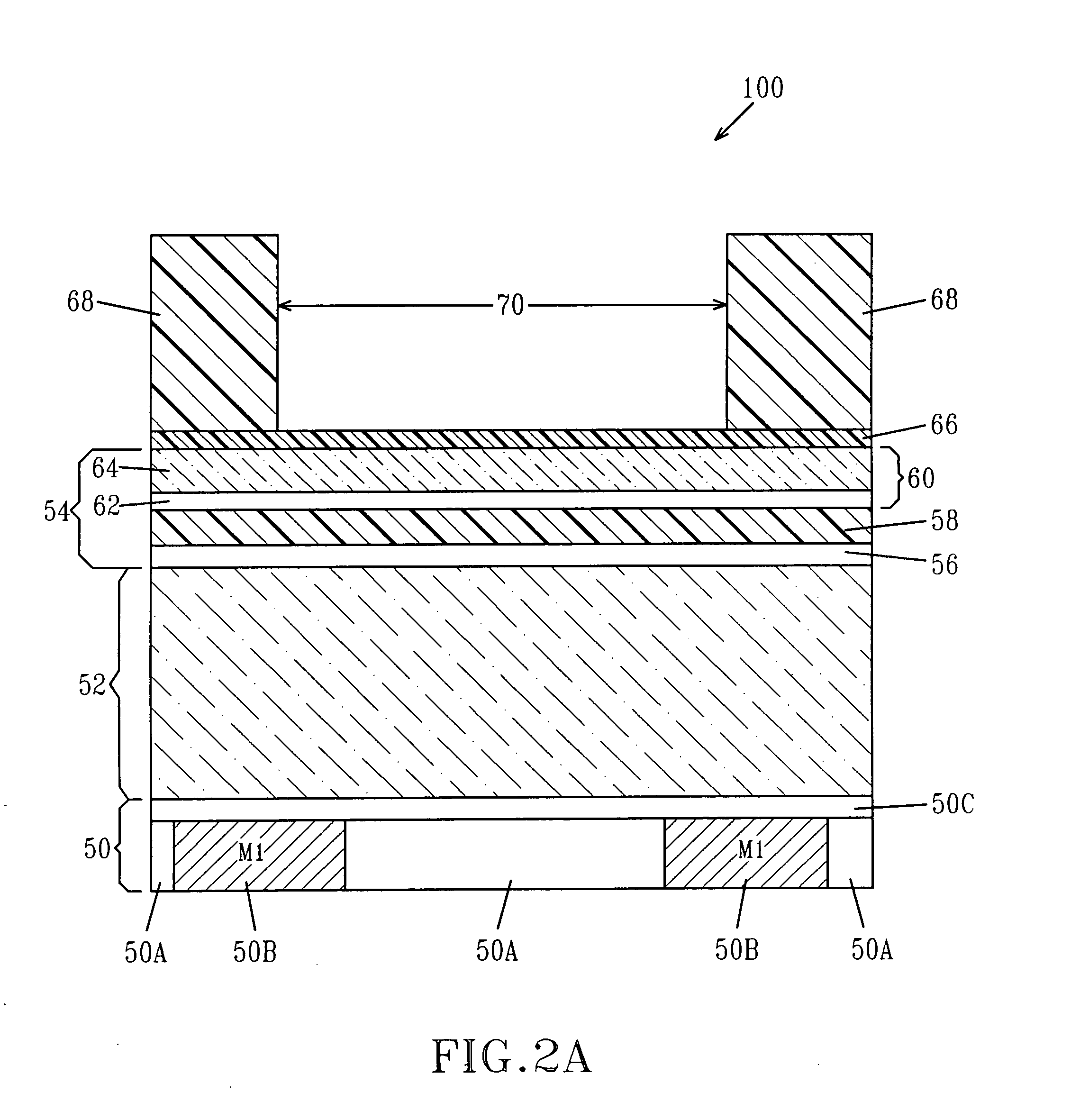
[0038] The present invention, which provides a multilayer hardmask technique for damage-free processing of OSG ILDs, will now be described in greater detail by referring to the drawings that accompany the present application. The drawings are provided herein for illustrative purposes and thus they are not drawn to scale.

[0039] The present invention which is directed to an interconnect structure useful for forming a semiconductor device, is such that a multilayer hardmask stack integration scheme is utilized to fabricate conductive / low-k interconnect structures of negligible plasma-induced dielectric modification and a substantial dual damascene process window. The interconnect structure of the present invention offers improved performance, reliability, and functionality. The integration scheme is such that an alternating hardmask stack scheme is employed including inorganic and organic type layers. Such a scheme in which the dual damascene process flow commences with definition of ...


PUM

PropertyMeasurementUnit
dielectric constantaaaaaaaaaa

Abstract

Interconnect structures possessing an organosilicate glass based material for 90 nm and beyond BEOL technologies in which a multilayer hardmask using a line-first approach are described. The interconnect structure of the invention achieves respective improved device/interconnect performance and affords a substantial dual damascene process window owing to the non-exposure of the OSG material to resist removal plasmas and because of the alternating inorganic/organic multilayer hardmask stack. The latter feature implies that for every inorganic layer that is being etched during a specific etch step, the corresponding pattern transfer layer in the field is organic and vice-versa.

Description

FIELD OF THE INVENTION [0001] The present invention generally relates to integrated circuits (ICs), and more particularly to interconnect structures, including multilevel interconnect structures, in which a multilayer hardmask patterning technique is employed to enable (i) negligible interlevel dielectric (ILD) modification (i.e., damage) during patterning and (ii) a sufficient dual damascene processing window; thus facilitating improved interconnect / device performance, reliability, and functionality. BACKGROUND OF THE INVENTION [0002] Generally, semiconductor devices include a plurality of circuits that form an IC including chips (e.g., chip back end of line, or “BEOL”), thin film packages and printed circuit boards. Integrated circuits can be useful for computers and electronic equipment and can contain millions of transistors and other circuit elements that are fabricated on a single silicon crystal substrate. For the device to be functional, a complex network of signal paths wil...

Claims


Application Information

Patent Timeline
Patent Type & Authority Applications(United States)
IPC IPC(8): B32B17/06B32B9/00H01L21/302
CPCH01L21/0331H01L21/76811H01L23/5329H01L23/53295Y10T428/12576H01L2924/0002Y10T428/12611H01L2924/00Y10T428/31667
Inventor FULLER, NICHOLAS C.M.GATES, STEPHEN MCCONNELLDALTON, TIMOTHY J.
Owner GLOBALFOUNDRIES US INC
Why Eureka
Try Eureka