A/d converter-incorporated solid-state imaging device

a solid-state imaging and converter technology, applied in the direction of code conversion, instruments, television systems, etc., can solve the problems increasing the man-hour needed, and difficult to send the test signal to the a/d converter b>7, so as to achieve the effect of increasing the test tim

Inactive Publication Date: 2009-11-19
PANASONIC CORP
View PDF6 Cites 12 Cited by
  • Summary
  • Abstract
  • Description
  • Claims
  • Application Information

AI Technical Summary

Benefits of technology

[0026]In the solid-state imaging device described above, in testing of the A / D converter, two signals, the first signal corresponding to the pixel reset signal level and the second signal corresponding to the pixel signal level, are inputted into the solid-state imaging device. The test signal selection circuit outputs the first signal and the second signal by selectively switching between the first and second signals to thereby generate a test signal having the first and second signals arranged in time series at desired timing. The resultant test signal is supplied to the A / D converter via the test signal input circuit. This configuration eliminates the necessity of providing a test signal generation circuit for generating the test signal having the first and second signals arranged in time series inside the solid-state imaging device. This further eliminates the necessity of testing for checking whether or not the test signal generated by the test signal generation circuit has desired precision for each solid-state imaging device. Hence, the problem of increasing the circuit scale and the problem of increasing the test time can be solved.

Problems solved by technology

As a result, it will be difficult to send the test signal TEST to the A / D converter 7 as a highly precise signal (second problem).
Also, a test for checking the precision of signals generated by the test signal generation circuit 12 is necessary for each solid-state imaging device, and this increases the test time (Fourth problem).
This increases both the man-hour needed to develop an IC tester satisfying this requirement and the cost required for this development (fifth problem).
However, for a solid-state imaging device in which an external clock is multiplied with a multiplication circuit to operate the A / D converter at high speed, as described in Patent Document 3, for example, it is difficult to synchronize the timing at which the reference signal and the amplitude signal are supplied to the solid-state imaging device 100 from the IC tester with the timing at which the reference signal and the amplitude signal are supplied to the A / D converter 7 (sixth problem).
It is therefore difficult to make the voltage value of the reference signal agree with the 0-point voltage value of the amplitude signal supplied from the IC tester.
As a result, high-precision testing with an amplitude signal having a small amplitude, in particular, will be difficult, causing a new problem.
This is however disadvantageous in that a test for checking the characteristics of the individual A / D converters is not allowed and that a test for checking variations among the A / D converters is not allowed.

Method used


Image

  • A/d converter-incorporated solid-state imaging device
  • A/d converter-incorporated solid-state imaging device
  • A/d converter-incorporated solid-state imaging device

Examples


embodiment 1

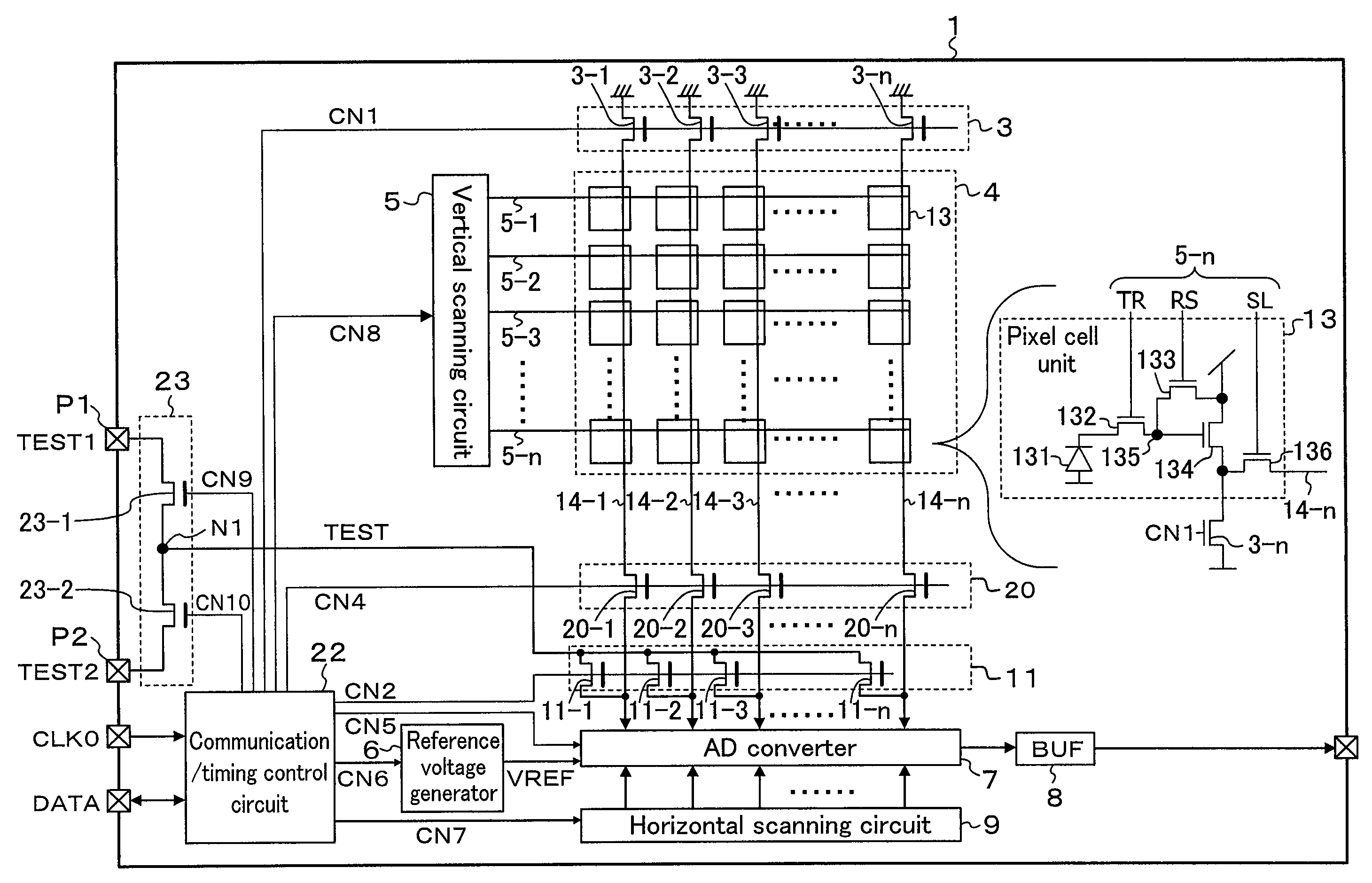
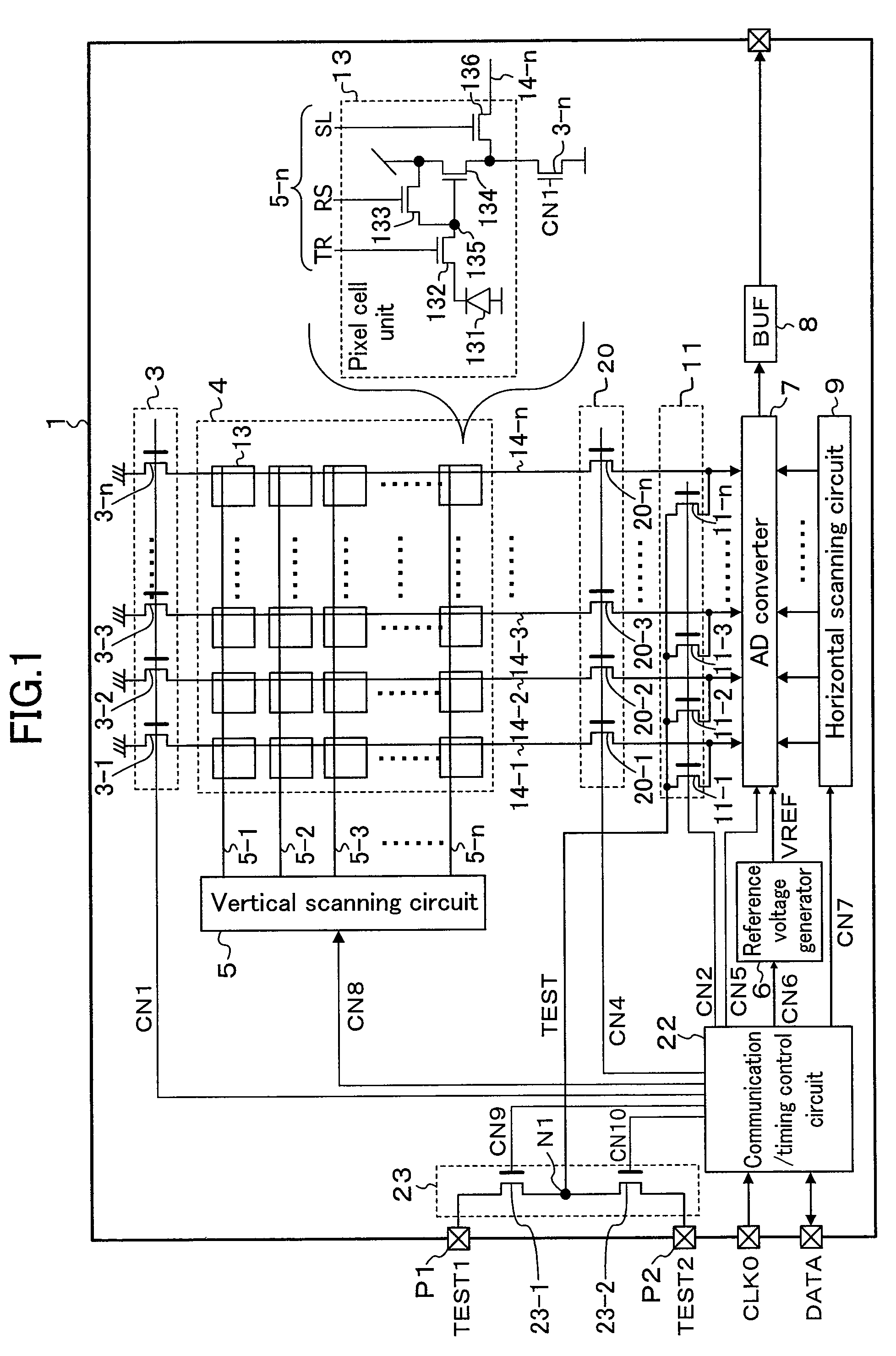
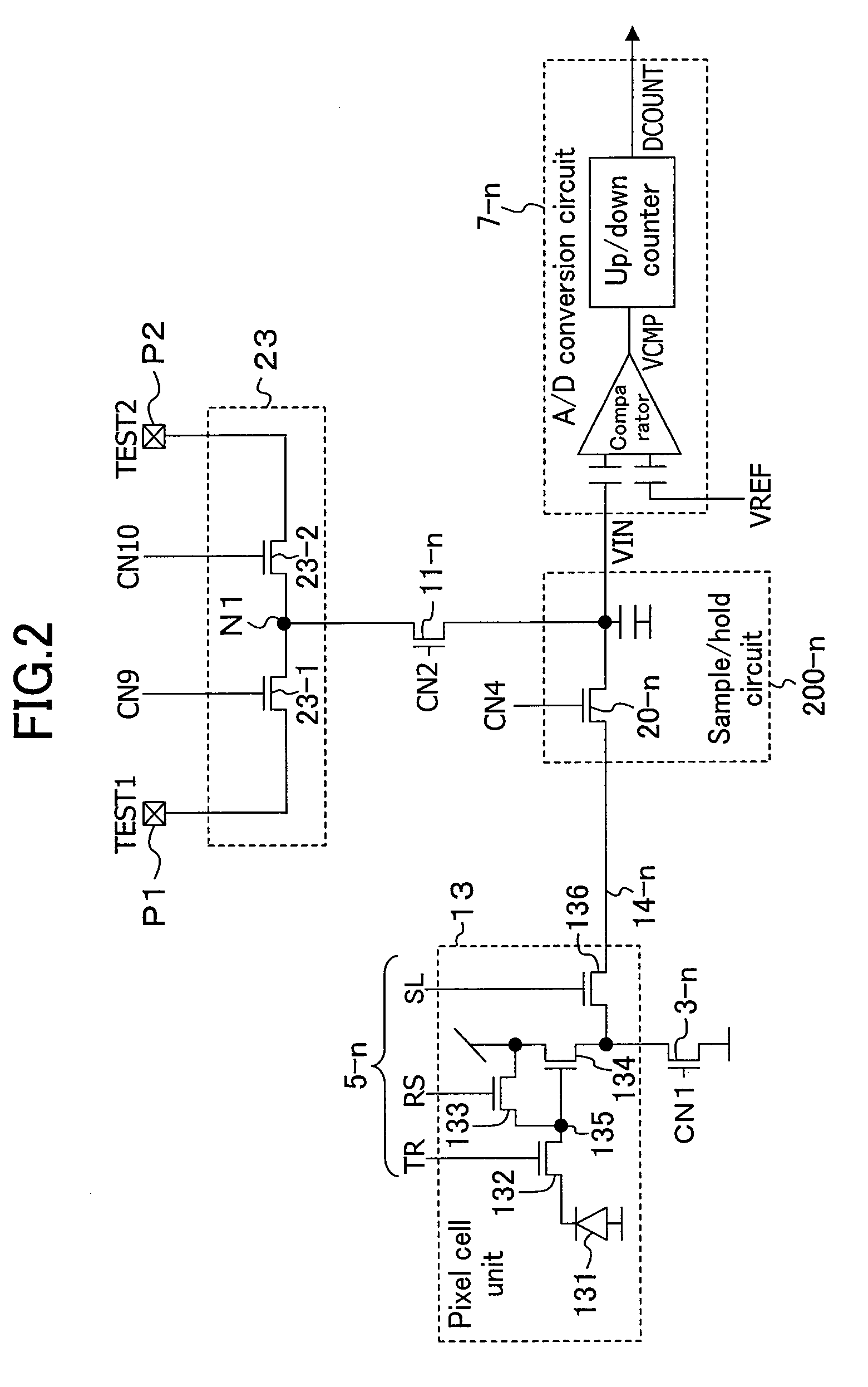
[0038]FIG. 1 is a block diagram of a solid-state imaging device of Embodiment 1. Referring to FIG. 1, the solid-state imaging device 1 includes a load transistor group 3, a pixel region 4, a vertical scanning circuit 5, a reference voltage generator 6, an A / D converter 7, a buffer (BUF) 8, a horizontal scanning circuit 9, a test signal input circuit 11, a vertical signal line connection circuit 20, a communication / timing control circuit 22 and a test signal selection circuit 23. These circuits are formed inside the solid-state imaging device 1 (on the same chip).

[0039]The pixel region 4 has a plurality of pixel cells 13 for converting light to signal charge arranged in a matrix. The plurality of pixel cells 13 are formed on a p-type substrate or in a P-well on an n-type substrate. Each pixel cell 13 includes a photodiode 131, a transfer transistor 132, a reset transistor 133, an amplifying transistor 134 and a pixel selection transistor 136. The photodiode 131 performs optoelectroni...

embodiment 2

[0066]In Embodiment 1, the test signal TEST outputted from the test signal selection circuit 23 was supplied to the A / D converter 7 via the test signal input circuit 11.

[0067]In such a solid-state imaging device that the A / D converter 7 thereof operates at low speed, however, the test signal TEST generated outside the solid-state imaging device may be supplied to the A / D converter 7 via the test signal input circuit 11 if no problem arises in the development of an IC tester that generates the reference signal and the amplitude signal at desired timing in a time-sharing manner and if the timing at which the reference signal and the amplitude signal are supplied from the IC tester to the solid-state imaging device can be synchronized with the timing at which these signals are supplied to the A / D converter 7. An example of such a solid-state imaging device will be described as follows as Embodiment 2.

[0068]FIG. 6 is a block diagram of a solid-state imaging device 60 of Embodiment 2. Mo...

embodiment 3

[0072]In Embodiments 1 and 2, the analog signals from the pixel cells 13 are given to the A / D converter 7 via the vertical signal lines (14-1 to 14-n) and the vertical signal line connection circuit 20.

[0073]In a solid-state imaging device in which the analog signals from the pixel cells 13 pass through an analog signal processing circuit that amplifies the analog signals, for example, before being given to the A / D converter 7, the vertical signal line connection circuit 20 and the test signal input circuit 11 must be placed so as to ensure that the test signal TEST is unaffected by the analog signal processing circuit.

[0074]In Embodiment 3, therefore, a solid-state imaging device having an analog signal processing circuit placed between the pixel region 4 and the A / D converter 7 will be described.

[0075]FIG. 7 is a block diagram of a solid-state imaging device70 of Embodiment 3. Most of the components in FIG. 7 are the same in function as the counterparts in FIG. 1. In this embodime...


PUM


Abstract

The solid-state imaging device includes: a first node for receiving a first signal from outside the solid-state imaging device; a second node for receiving a second signal from outside the solid-state imaging device; a test signal selection circuit for outputting the first signal received at the first node and the second signal received at the second node as a test signal by switching between the first and second signals at desired timing; and a test signal input circuit for supplying the test signal from the test signal selection circuit to an input of the A / D converter.

Description

CROSS-REFERENCE TO RELATED APPLICATIONS[0001]This application claims priority under 35 U.S.C. §119 on Patent Application No. 2008-125852 filed in Japan on May 13, 2008, the entire contents of which are hereby incorporated by reference.BACKGROUND OF THE INVENTION[0002]The present invention relates to a solid-state imaging device incorporating an A / D converter, and more particularly to a solid-state imaging device having a function for testing of the A / D converter. The present invention is applied to CMOS image sensors used for image sensor-embedded cellular phones, digital cameras, video cameras and the like, for example.[0003]In recent years, various schemes have been proposed for signal readout in solid-state imaging devices. In general, a column parallel output type solid-state imaging device is often used in which one row of pixels in a pixel array are selected and pixel signals generated in the selected pixels are read in parallel via vertical signal lines. Also, a solid-state i...

Claims


Application Information

Patent Timeline
Patent Type & Authority Applications(United States)
IPC IPC(8): H04N5/335H03M1/10H04N5/374H04N5/3745H04N5/378
CPCH03M1/108H03M1/123H04N17/002H04N5/37455H03M1/56H04N25/772
Inventor NAKAO, TOSHINOBUHIROTA, MASAYUKIMURAKAMI, MASASHIWATANABE, KENJIHIROSE, MASAYA
Owner PANASONIC CORP
Why Eureka
Try Eureka