

Light emitting device package
a technology of light-emitting devices and light-emitting devices, which is applied in the direction of semiconductor devices, basic electric elements, electrical equipment, etc., can solve the problems of color deviation and light efficiency reduction, and achieve the effect of improving light efficiency and reducing color deviation
- Summary
- Abstract
- Description
- Claims
- Application Information
AI Technical Summary
Benefits of technology
Problems solved by technology
Method used
Image

Examples
first embodiment
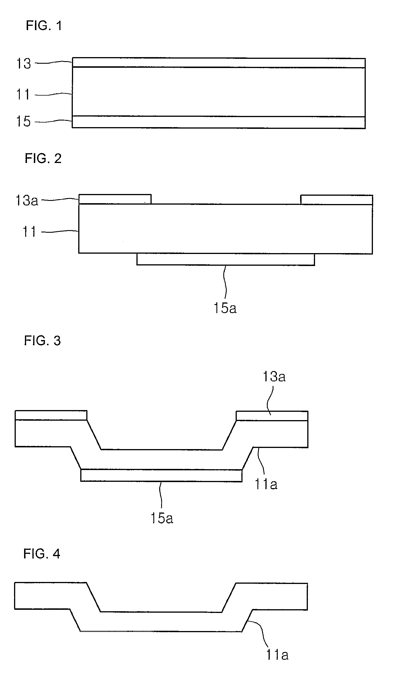
[0020]FIGS. 1 to 11 are sectional views showing the manufacturing process of a light emitting device package according to a first embodiment.
[0021]First, as shown in FIG. 1, first and second masks 13 and 15 are formed on upper and lower surfaces of a semiconductor substrate 11.
[0022]Next, as shown in FIG. 2, in order to etch the semiconductor substrate 11, a first pattern mask 13a and a second pattern mask 15a are formed. The first and second pattern masks 13a and 15a can be formed through a photolithography process.
[0023]The semiconductor substrate 11 can include single crystalline silicon, but the embodiment is not limited thereto. The semiconductor substrate 11 can be etched through a dry etching process or a wet etching process. When the semiconductor substrate 11 includes a silicon substrate, the first and second masks 13 and 15 can include a silicon nitride layer, but the embodiment is not limited. In addition, the semiconductor substrate 11 can be subject to a KOH wet etching...
second embodiment
[0046]FIG. 12 is a sectional view showing a light emitting device package according to a second embodiment.
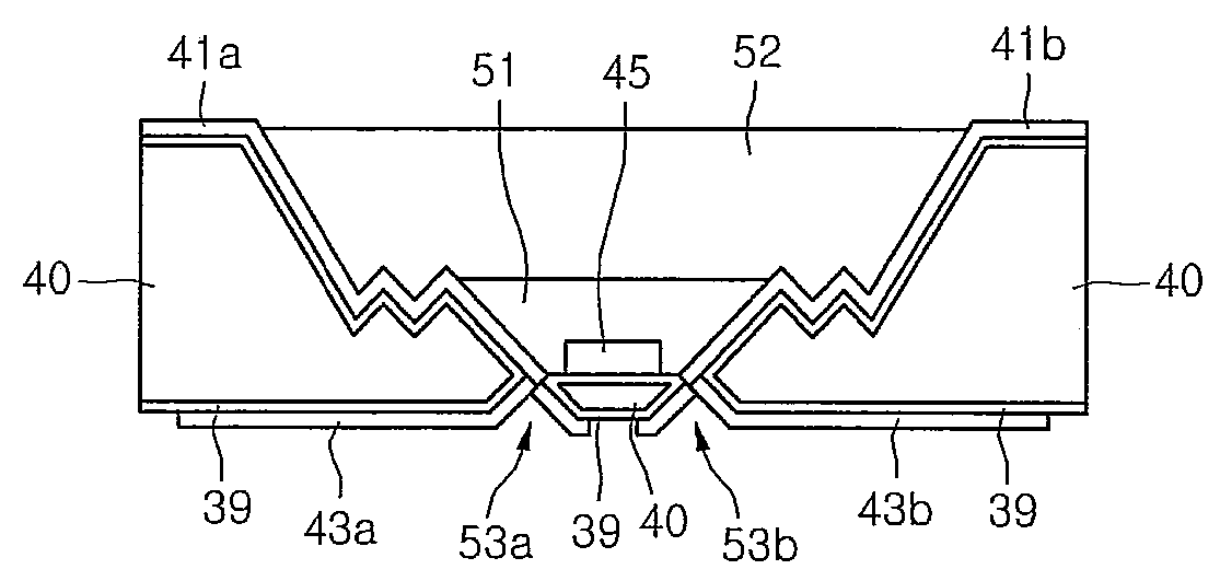
[0047]The light emitting device package according to the second embodiment includes the second semiconductor substrate 11b, the light emitting part 25, the first metal layer 21a, the second metal layer 21b, the third metal layer 23a, the fourth metal layer 23b, a first molding part 31, a second molding part 32, and the insulating layer 19.
[0048]The second embodiment can employ the technical features of the first embodiment, so the second embodiment will be described while focusing on the features distinguished from the first embodiment.
[0049]Different from the first embodiment, according to the second embodiment, a phosphor is provided in the second molding part 32. For example, the first molding part 31 can be formed on the light emitting part 25, and the second molding part 32 can be formed on the first molding part 31. The second molding part 32 can include a second phosphor...
third embodiment
[0051]FIG. 13 is a sectional view showing a light emitting device package according to a third embodiment.
[0052]The third embodiment can employ the technical features of the first embodiment, so that the third embodiment will be described while focusing on the features distinguished from the first embodiment.
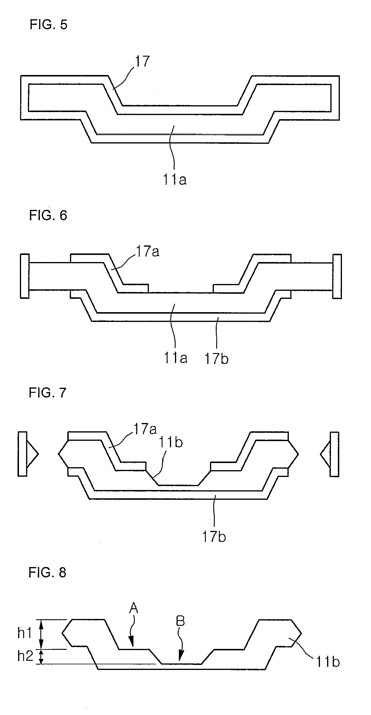
[0053]When compared to the first embodiment, the third embodiment employs a third semiconductor substrate 11c having a first surface in a concave-convex shape. For example, when a second surface of the third semiconductor substrate 11c is formed, the second surface having the second depth is formed in a second region of the first surface, and a third surface having a concave-convex shape is formed in a third region of the first surface, thereby forming the third semiconductor substrate 11c having a concave-convex shape as shown in FIG. 13. The concave-convex shape can include a V-shape groove, but the embodiment is not limited thereto.
[0054]According to the third embodiment, the...
PUM
 Abstract
Description
Claims
Application Information