Impedance calibration circuit, semiconductor memory device with the impedance calibration circuit and layout method of internal resistance in the impedance calibration circuit

a calibration circuit and impedance technology, applied in the field of semiconductor memory devices with impedance calibration circuits, can solve the problems of generate impedance mismatch, detect and calibrate, and impedance mismatch between the impedance calibration circuit and the data i/o driver, and achieve the effect of easy calibration of impedance mismatch

Inactive Publication Date: 2009-11-26
SK HYNIX INC
View PDF11 Cites 22 Cited by
  • Summary
  • Abstract
  • Description
  • Claims
  • Application Information

AI Technical Summary

Benefits of technology

[0040]The present invention provides an impedance calibration circuit including internal resistances having at least one variable resistance. Therefore, it is possible to easily calibrate impedance mismatch between the impedance calibration circuit and a data I/O driver.
[0041]Also, the present invention provides a semiconductor memory device in which at least one of the internal resistances of an impedance calibration circuit is a variable resistance. Therefore, it is possibl...

Problems solved by technology

However, the structure of conventional semiconductor memory devices tends to cause an impedance mismatch between the impedance calibration circuit and the data I/O driver.
It is difficult to detect and calibrate for this impedance mismatch, and therefore the generated impedance mismatch can be problematic.
Therefore, in a conventional semiconductor memory device there is a high probability that an impedance mismatch will occur, since the legs of the impedance calibration circuit and the legs of the data I/O driver have different layout structures.
The difference in structure of the connection to an ext...

Method used


Image

  • Impedance calibration circuit, semiconductor memory device with the impedance calibration circuit and layout method of internal resistance in the impedance calibration circuit
  • Impedance calibration circuit, semiconductor memory device with the impedance calibration circuit and layout method of internal resistance in the impedance calibration circuit
  • Impedance calibration circuit, semiconductor memory device with the impedance calibration circuit and layout method of internal resistance in the impedance calibration circuit

Examples


Embodiment Construction

[0049]Hereinafter, preferred embodiments of the present invention will be described in detail with reference to the accompanying drawings.

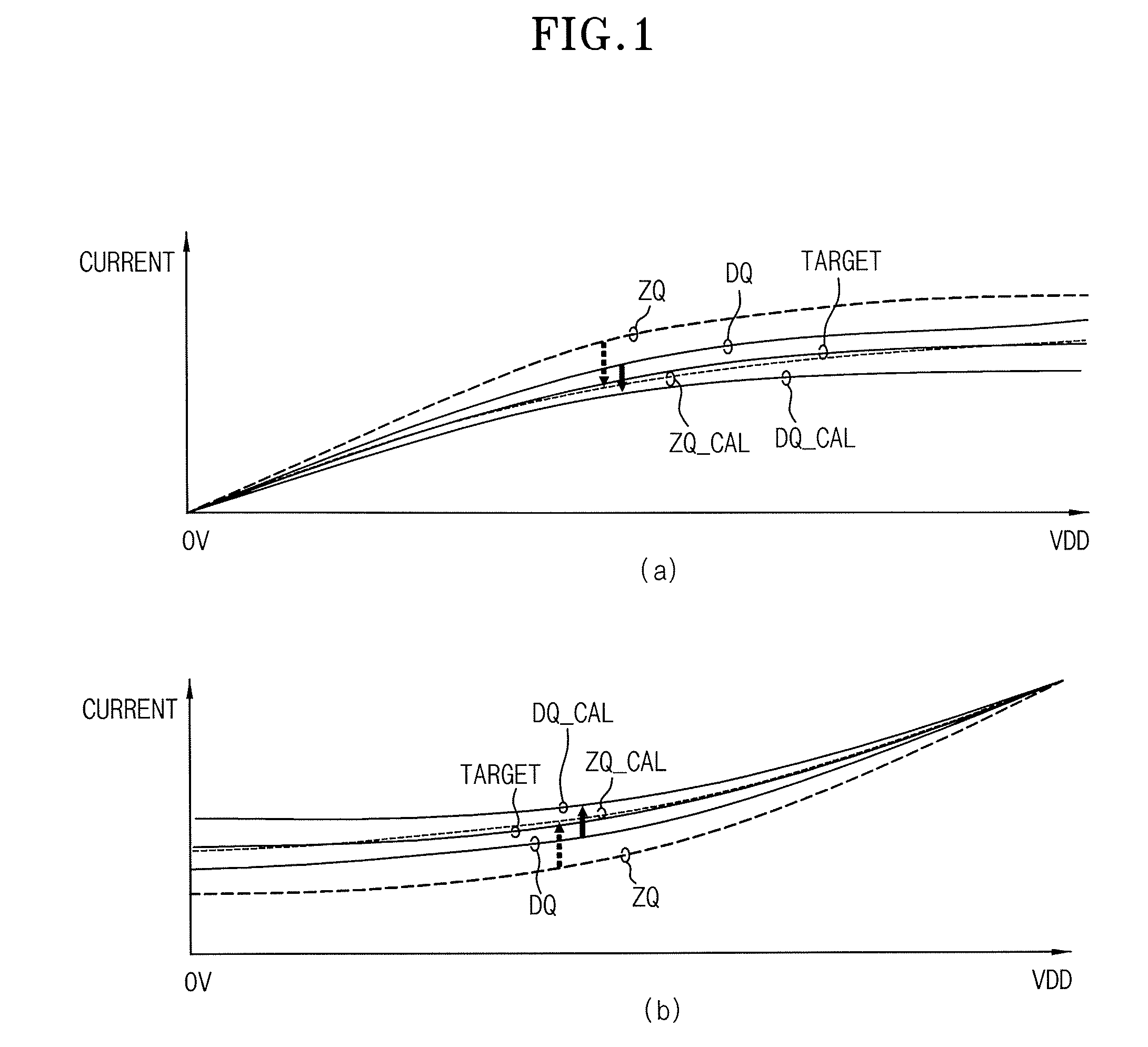
[0050]The present invention discloses an impedance calibration circuit that can vary the resistance value of at least one of a plurality of internal resistances for impedance matching with the I / O impedance of an external device, and a semiconductor memory device having the same.

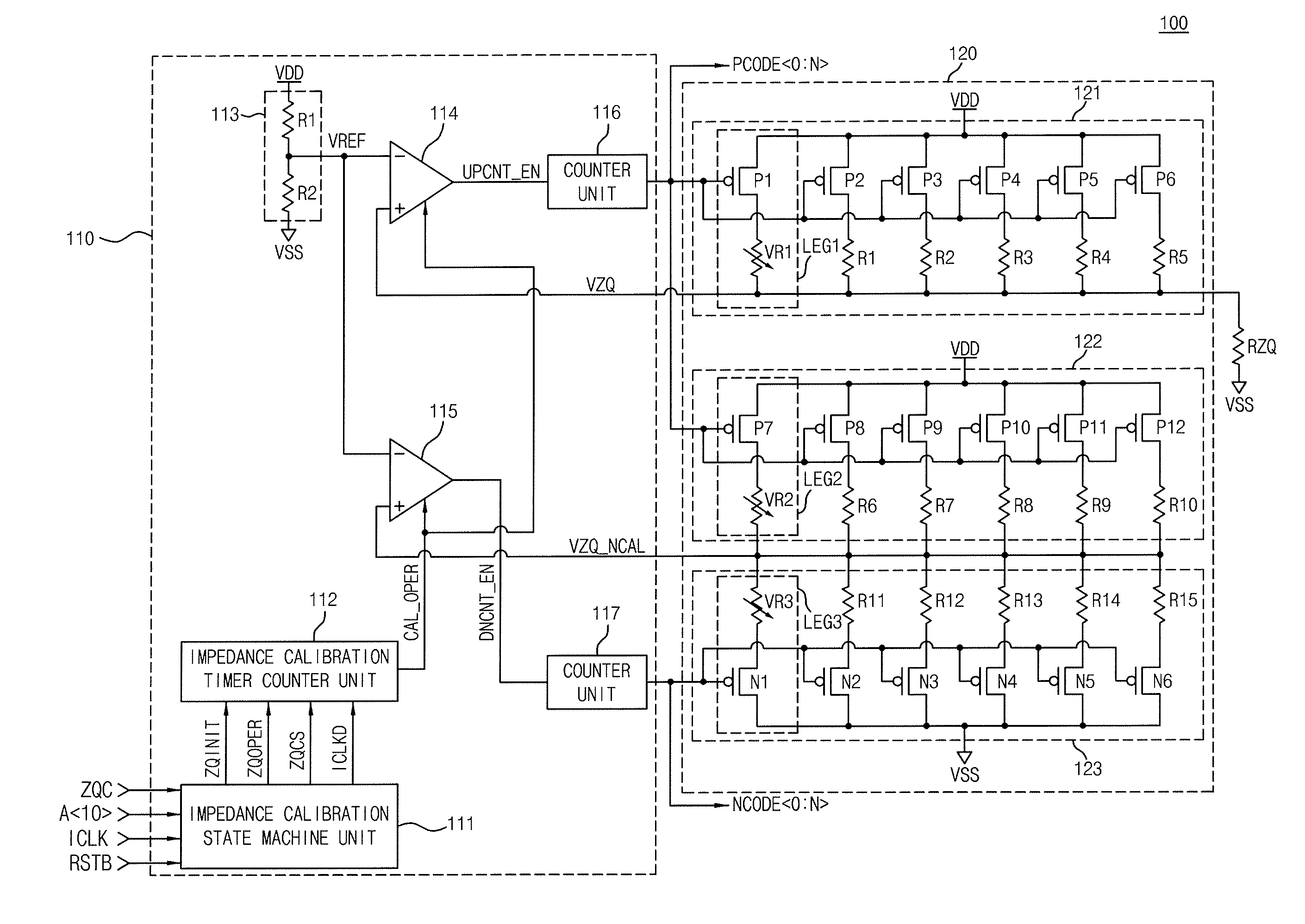
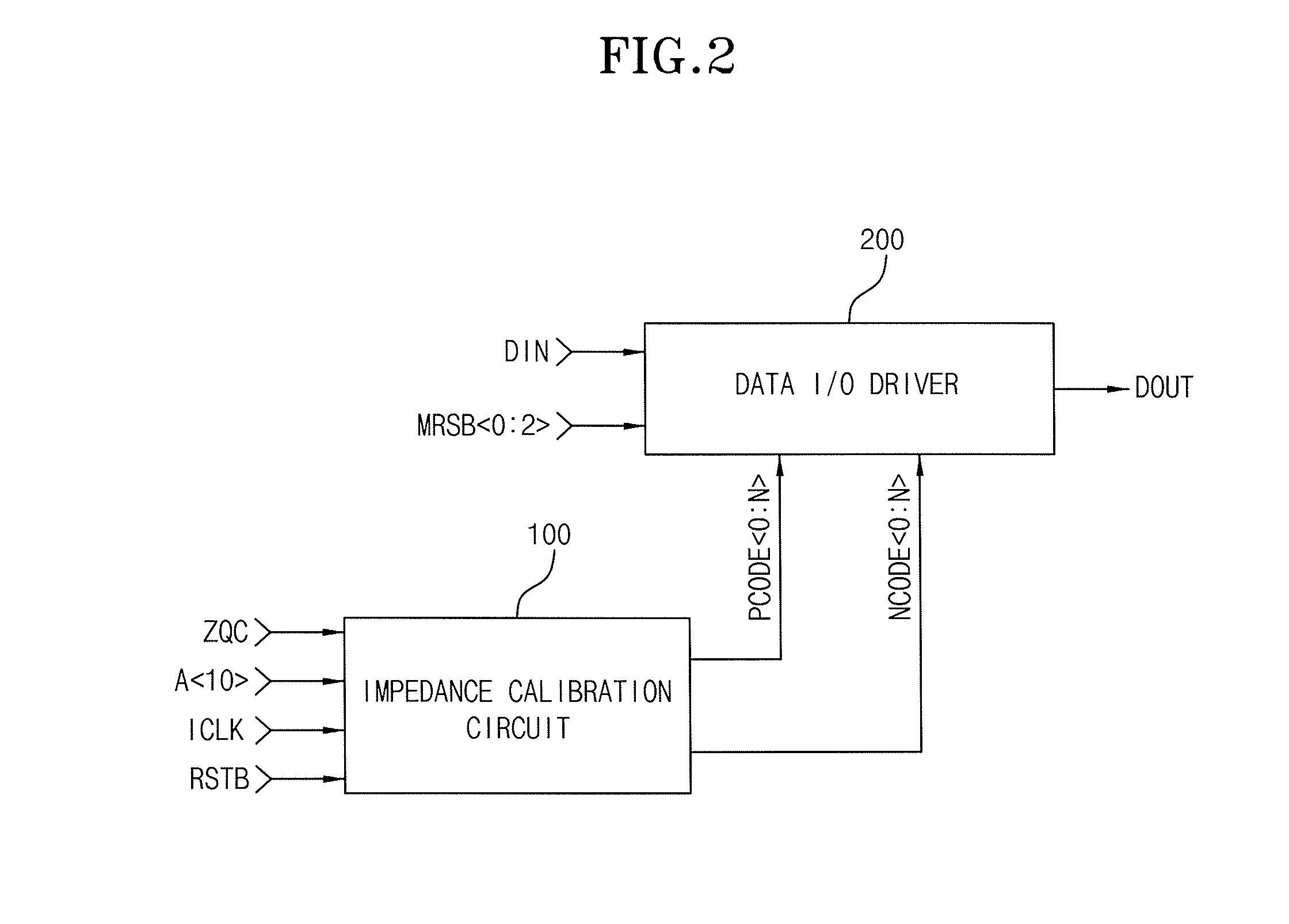
[0051]Referring to FIG. 2, a semiconductor memory device according to an embodiment of the present invention includes an impedance calibration circuit 100 and a data I / O driver 200.

[0052]The impedance calibration circuit 100 receives a command signal ZQC, an address signal A10>, an internal clock ICLK, and a reset signal RSTB used to determine an impedance calibration time. The impedance calibration circuit 100 compares the impedance of resistances (not shown) provided therein to the impedance of an external resistance (not shown) corresponding to an I / O impedance of an ex...


PUM


Abstract

An impedance calibration circuit for impedance matching between a semiconductor memory device and an external device includes a driving circuit and a comparing circuit. The driving circuit has a plurality of internal resistances, with one or more of the internal resistances being a variable resistance. The driving circuit compares the impedance of the internal resistances to the input/output impedance of the external device in order to provide a calibration voltage. The comparing circuit compares the calibration voltage to a reference voltage and provides a code signal for calibrating the impedance corresponding to output data with the input/output impedance of the external device. The impedance calibration circuit calibrates an impedance mismatch between the impedance calibration circuit and a data input/output driver by adjusting the impedance of the impedance calibration circuit through the variable resistance.

Description

CROSS-REFERENCE TO RELATED APPLICATIONS[0001]The present application claims priority to Korean patent application number 10-2008-0047391 filed on May 22, 2008, which is incorporated herein by reference in its entirety.BACKGROUND OF THE INVENTION[0002]The present invention relates generally to a semiconductor memory device, and more particularly, to an impedance calibration circuit for impedance matching between a semiconductor memory device and an external device, a semiconductor memory device including the impedance calibration circuit at an input / output terminal thereof, and a layout method of an internal resistance in the impedance calibration circuit.[0003]Typically, a high speed semiconductor memory device such as a DDR3 is provided with an impedance calibration circuit that calibrates an on die termination (ODT) value in response to process, voltage, and temperature (PVT) variation.[0004]The impedance calibration circuit calibrates the impedance of an internal resistance by ut...

Claims


Application Information

Patent Timeline
IPC IPC(8): H03K17/16
CPCG11C5/063G11C7/1051H03K19/0005G11C2207/2254G11C7/1057G11C7/1048H03K19/017545H04L25/0278
Inventor MOON, IN JUN
Owner SK HYNIX INC
Why Eureka
Try Eureka