Inspecting Method and Inspecting Apparatus for Substrate Surface

Active Publication Date: 2009-11-26
HITACHI HIGH-TECH CORP
View PDF3 Cites 30 Cited by
  • Summary
  • Abstract
  • Description
  • Claims
  • Application Information

AI Technical Summary

Benefits of technology

[0005]As the degree of integration of the semiconductor product is increased, it is required that the surface inspection of the substrate has the higher sensi

Problems solved by technology

However, in the optical inspecting apparatuses as disclosed in the above documents, the inspection for the microroughnes

Method used


Image

  • Inspecting Method and Inspecting Apparatus for Substrate Surface
  • Inspecting Method and Inspecting Apparatus for Substrate Surface
  • Inspecting Method and Inspecting Apparatus for Substrate Surface

Examples


Embodiment Construction

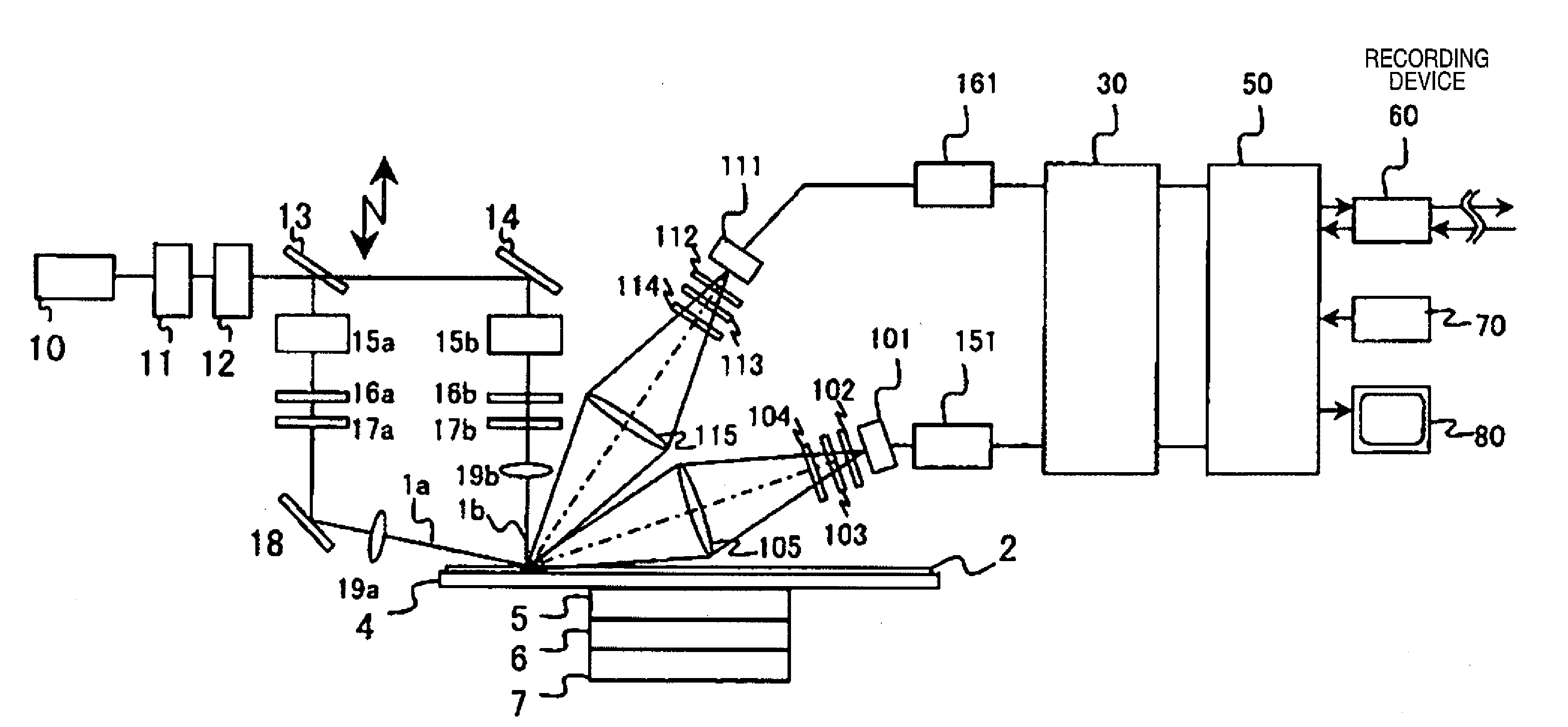
[0062]The embodiments of the present invention will be described below by exemplifying an inspecting apparatus that detects a defect on the surface of a wafer without pattern formed (bare wafer, or wafer in which bare wafer is subjected to a film formation process, a washing process, or a polishing process).

[0063]The inspecting apparatus according to the invention appropriately comprises an illuminating optical system 1001 for applying light to a substrate of inspection object, a stage scanning section 1003 for inspecting all or part of the substrate, a detecting optical system 1002 for detecting the scattered light or reflected light, a signal processing section 1004 for determining the defect or haze, and a data processing control section 50 for making the post-processing for the detected defect or haze. Each configuration will be specifically described below.

[0064]The illuminating optical system 1001 as shown in FIG. 1 has an obliquely illuminating optical system for applying an ...


PUM


Abstract

To inspect a substrate such as a semiconductor substrate for surface roughness at high precision.
The surface roughness of the substrate is measured in each frequency band of the surface roughness by applying a light to the substrate surface and detecting a scattered light or reflected light at a plurality of azimuth or elevation angles.

Description

BACKGROUND OF THE INVENTION [0001]The present invention relates to an inspecting method and an inspecting apparatus for inspecting the surface roughness existing on the surface of a substrate such as a semiconductor substrate or a hard disk substrate.[0002]In a manufacturing line for the semiconductor substrate or thin film substrate, the inspection for defect or foreign matter existing on the surface of the semiconductor substrate or thin film substrate is made to maintain and improve the yields of products. For example, in a sample such as a semiconductor substrate before forming a circuit pattern, it is required to detect a microscopic defect or foreign matter (hereinafter called a defect) of 0.05 μm or less on the surface or microroughness (haze) on the surface. Also, to detect such defect, the conventional inspecting apparatus applies a condensed laser beam to the surface of the sample and condenses and detects a scattered light from the defect. Also, in a sample such as a semi...

Claims


Application Information

Patent Timeline
IPC IPC(8): G01B11/30G01B11/06
CPCG01B11/303G01N21/9501G01N21/94G01N21/47
Inventor HAMAMATSU, AKIRAOSHIMA, YOSHIMASAMAEDA, SHUNJISHIBUYA, HISAEURANO, YUTANAKAO, TOSHIUKIMARUYAMA, SHIGENOBU
Owner HITACHI HIGH-TECH CORP
Why Eureka
Try Eureka