Solid-State Image Pickup Device

a solid-state image and pickup device technology, applied in the direction of color signal processing circuits, television systems, radio control devices, etc., can solve the problems of low luminance region dynamic range, low resolution, and low quantity efficiency, and achieve the effect of high luminance region

Active Publication Date: 2009-12-03
TEXAS INSTR JAPAN
View PDF3 Cites 82 Cited by
  • Summary
  • Abstract
  • Description
  • Claims
  • Application Information

AI Technical Summary

Benefits of technology

[0023]The solid-state image pickup device of the present invention includes an additional capacitance capacitance-separated from flo...

Problems solved by technology

When using color filters of different colors for each pixel in a single-plate color image sensor the quantum efficiency drops due to attenuation.
Since the white pixels are saturated at lower luminance than the red, green and blue pixels with low quantum efficiency in the high luminanc...

Method used


Image

  • Solid-State Image Pickup Device
  • Solid-State Image Pickup Device
  • Solid-State Image Pickup Device

Examples


first embodiment

[0063]The solid-state image pickup device disclosed in this embodiment is a CMOS image sensor. White pixels having no color filter, and red pixels, green pixels and blue pixels having corresponding red, green, and blue color filters are integrated in an array on the light receiving surface of a semiconductor substrate.

[0064]In the CMOS image sensor disclosed in this embodiment, the white pixels, red pixels, green pixels and blue pixels have a common circuit configuration and differ from each other in presence / absence and colors of corresponding color filters.

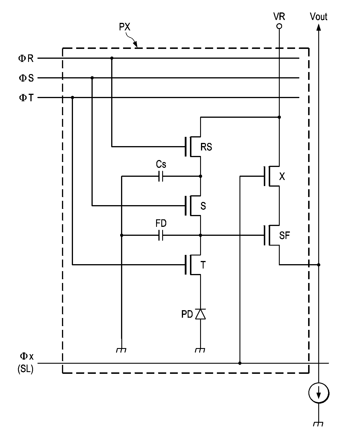
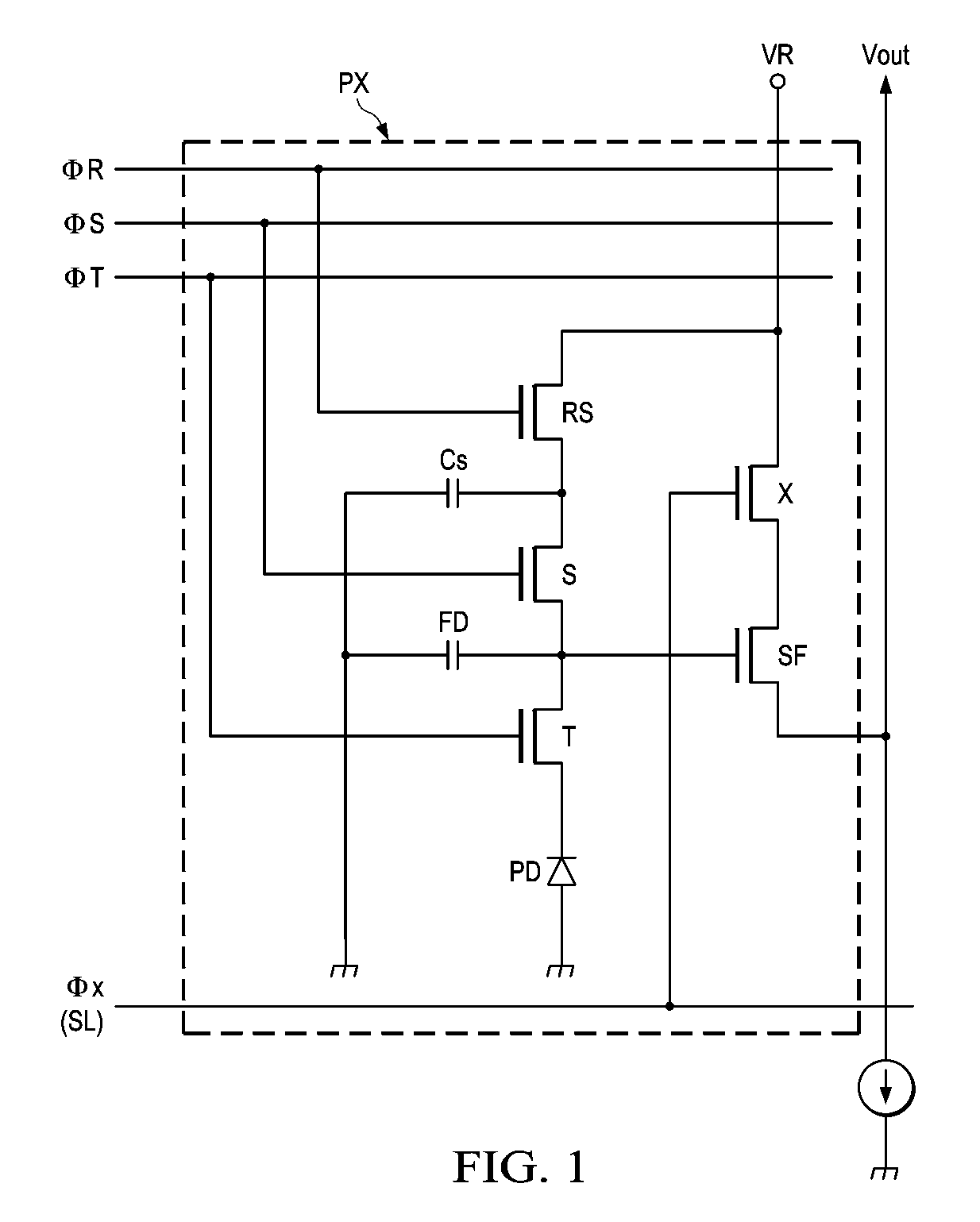
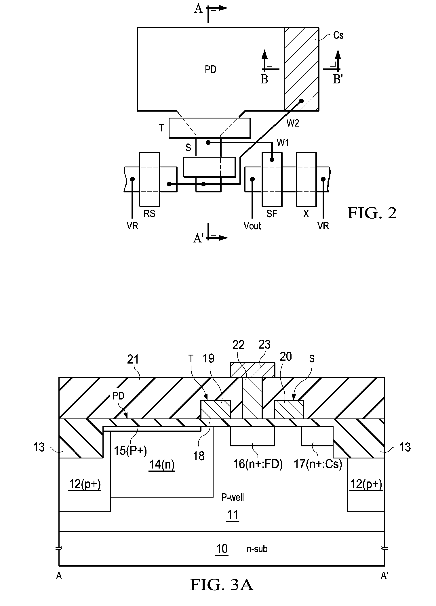
[0065]FIG. 1 is an equivalent circuit diagram of one pixel (pixel) PX.

[0066]Each pixel includes: photodiode PD that receives light to generate and accumulate photocharges; transfer transistor T that transfers the photocharges from photodiode PD; floating diffusion FD which receives the transferred photocharges via transfer transistor T; additional capacitance CS; capacitance-coupling transistor S that selectively couples or sepa...

second embodiment

[0145]The solid-state image pickup device of this embodiment is a CMOS image sensor. White pixels having no color filter, red pixels having red color filters, green pixels having green color filters and blue pixels having blue color filters are integrated in array form on the light receiving surface of a semiconductor substrate.

[0146]In this embodiment, the additional capacitance included in white pixels is larger than the additional capacitance included in red pixels, green pixels and blue pixels.

[0147]The rest of the image sensor is virtually the same as in the first embodiment.

[0148]In the CMOS image sensor of this embodiment, an additional capacitance having the configuration to be described below and included in white pixels is larger than the additional capacitance included in red pixels, green pixels and blue pixels.

[0149]FIG. 13 is a layout diagram illustrating the state in which a group of four pixels (PX1 to PX4) of white pixel W, red pixel R, green pixel G and blue pixel ...

third embodiment

[0178]The solid-state image pickup device of this embodiment is a CMOS image sensor. White pixels having no color filter and red pixels, green pixels and blue pixels having corresponding red, green and blue color filters are integrated in array form on the light receiving surface of a semiconductor substrate.

[0179]In this embodiment, the number of white pixels W is greater than or equal to the total number of red pixels R, green pixels G and blue pixels B. The rest of the image sensor is virtually the same as in the first embodiment.

[0180]FIG. 18(A) is a layout diagram illustrating 16 pixels arranged in 4 rows by 4 columns as an example of the CMOS image sensor of this embodiment.

[0181]The ratio of the number of white pixels to the total number of red pixels R, green pixels G and blue pixels B is 3:1. A first 2 by 2 group of pixels includes red pixel PX1a and white pixels PX2a, PX3a and PX4a. A second 2 by 2 group of pixels includes green pixel PX2a and three white pixels PX2b, PX3b...


PUM


Abstract

This invention is a solid-state image pickup device that solves the problem of limited dynamic range in the high luminance region in an image sensor having white pixels. White pixels or yellow pixels and at least red pixels, green pixels or blue pixels are arranged in array form on the light receiving surface of a semiconductor substrate. White pixels or yellow pixels have an additional capacitance CS connected to the photodiode via the floating diffusion, a capacitance coupling transistor S that can couple or separate the floating diffusion and the additional capacitance. The proportion of white or yellow pixels to the total number of pixels is higher in a central portion of the light receiving surface than a peripheral portion. The white or yellow pixel may share a floating diffusion with a red, green or blue pixel.

Description

CLAIM OF PRIORITY[0001]This application claims priority under 35 U.S.C. 119(a) to Japanese Patent Application No. 2008-167304 filed May 20, 2008.TECHNICAL FIELD OF THE INVENTION[0002]The technical field of this invention is a solid-state pickup device and particularly a CMOS type or CCD type solid-state image pickup device.BACKGROUND OF THE INVENTION[0003]The characteristics of a CMOS (complementary metal-oxide-semiconductor) image sensor or a CCD (charge coupled device) image sensor and other image input image sensors have been improved. The demand for these image sensors is growing in various application fields such as digital cameras or camera-incorporated cellular phones.[0004]FIG. 33 shows the spectral sensitivity of an image sensor when using an IR ray eliminating filter rays and using various color filters on the silicon photodiodes that constitutes pixels of the image sensor in terms of light detection levels versus wavelength in Angstroms. The line marked R represents the s...

Claims


Application Information

Patent Timeline
IPC IPC(8): H04N5/335H01L27/146H04N5/355H04N5/357H04N5/369H04N5/372H04N5/374
CPCH04N5/3559H04N9/045H04N5/37457H04N5/37452H04N25/59H04N25/778H04N25/771
Inventor OSHIKUBO, HIROMICHADACHI, SATORUMIZOBUCHI, KOICHI
Owner TEXAS INSTR JAPAN
Why Eureka
Try Eureka