Transmission circuit for bias control of power amplifier
a power amplifier and bias control technology, applied in pulse technique, phase-modulated carrier system, baseband system details, etc., can solve the problem that the power amplifier b>504/b> cannot be prevented from entering a non-bias state, and achieve the effect of preventing the output signal, conducting the switching of operation mode, and high efficiency
- Summary
- Abstract
- Description
- Claims
- Application Information
AI Technical Summary
Benefits of technology
Problems solved by technology
Method used
Image

Examples
first embodiment
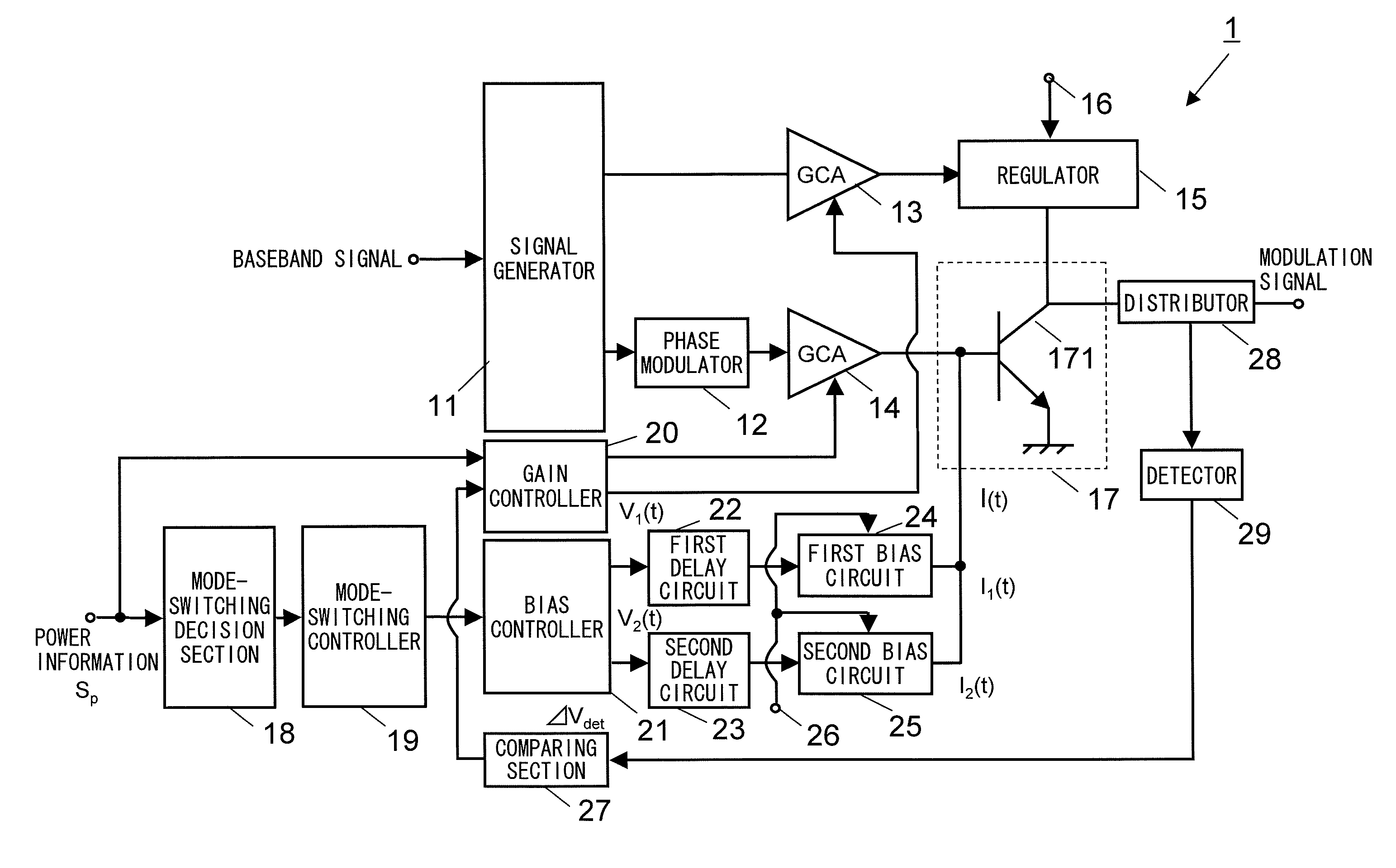
[0042]FIG. 1 is a block diagram showing one configuration example of a transmission circuit 1 according to a first embodiment of the present invention. The transmission circuit 1 in FIG. 1 includes: a signal generator 11; a phase modulator 12; a first variable gain amplifier (GCA) 13; a second variable gain amplifier (GCA) 14; a regulator 15; a power supply terminal 16; a power amplifier 17; a mode-switching decision section 18; a mode-switching controller 19; a gain controller 20; a bias controller 21; a first delay circuit 22; a second delay circuit 23; a first bias circuit 24; a second bias circuit 25; a power supply terminal 26; a comparing section 27; a distributor 28; and a detector 29. The power amplifier 17 includes a transistor for amplification 171.
[0043]In the transmission circuit 1, the signal generator 11 conducts a predefined signal processing on a baseband signal, and generates an amplitude signal and a phase signal. The amplitude signal is inputted into the regulator...
second embodiment
[0077]FIG. 5 is a block diagram showing one configuration example of a transmission circuit 2 according to a second embodiment of the present invention. The transmission circuit 2 in FIG. 5 includes: the signal generator 11; the phase modulator 12; the first variable gain amplifier (GCA) 13; the second variable gain amplifier (GCA) 14; the regulator 15; the power supply terminal 16; the power amplifier 17; a mode-switching decision section 58; a mode-switching controller 59; a gain controller 60; the bias controller 21; the first delay circuit 22; the second delay circuit 23; the first bias circuit 24; the second bias circuit 25; the power supply terminal 26; a comparing section 67; the distributor 28; and a detector 69. The power amplifier 17 includes the transistor for amplification 171.
[0078]When compared to the transmission circuit 1 according to the first embodiment, the characteristic of the transmission circuit 2 according to the second embodiment is conducting the operation ...
third embodiment
[0097]FIG. 9 is a block diagram showing one configuration example of a communication device according to a third embodiment of the present invention. The communication device 200 according to the third embodiment in FIG. 9 includes: a transmission circuit 210; a reception circuit 220; an antenna duplexer 230; and an antenna 240. The transmission circuit 210 is the transmission circuit described above in either the first or the second embodiment. The antenna duplexer 230 transmits a transmission signal outputted from the transmission circuit 210 to the antenna 240, and prevents the transmission signal from leaking into the reception circuit 220. Furthermore, the antenna duplexer 230 transmits a reception signal inputted from the antenna 240 to the reception circuit 220, and prevents the reception signal from leaking into the transmission circuit 210. As a result, the transmission signal is outputted from the transmission circuit 210 and released out into open space from the antenna 2...
PUM
 Abstract
Description
Claims
Application Information
 - R&D
- Intellectual Property
- Life Sciences
- Materials
- Tech Scout
- Unparalleled Data Quality
- Higher Quality Content
- 60% Fewer Hallucinations
Browse by: Latest US Patents, China's latest patents, Technical Efficacy Thesaurus, Application Domain, Technology Topic, Popular Technical Reports.
© 2025 PatSnap. All rights reserved.Legal|Privacy policy|Modern Slavery Act Transparency Statement|Sitemap|About US| Contact US: help@patsnap.com