
Transmission circuit for bias control of power amplifier

a power amplifier and bias control technology, applied in pulse technique, phase-modulated carrier system, baseband system details, etc., can solve the problem that the power amplifier b>504/b> cannot be prevented from entering a non-bias state, and achieve the effect of preventing the output signal, conducting the switching of operation mode, and high efficiency

Active Publication Date: 2012-07-17
PANASONIC CORP
View PDF4 Cites 7 Cited by
  • Summary
  • Abstract
  • Description
  • Claims
  • Application Information

AI Technical Summary

Benefits of technology

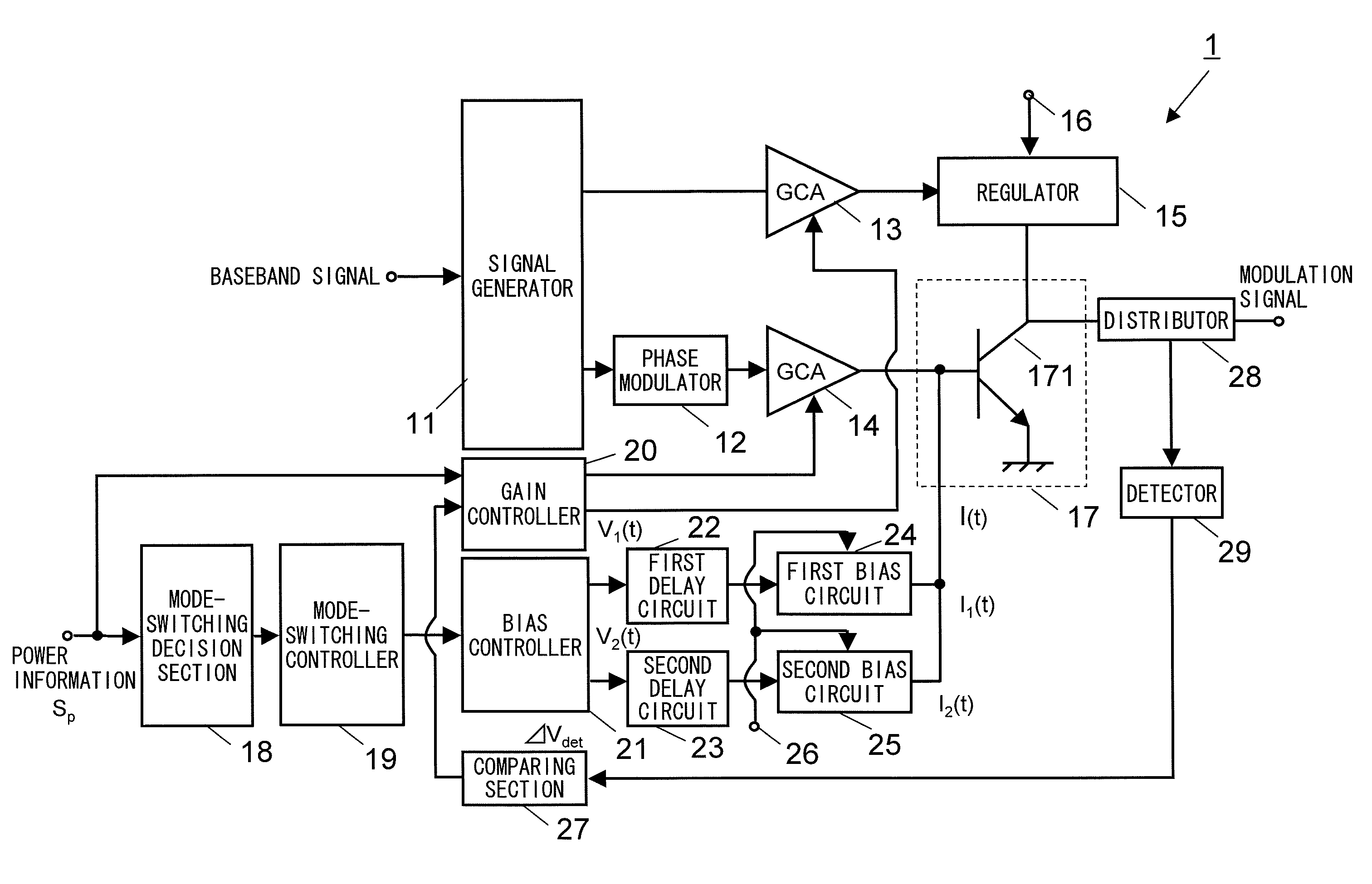
"The present invention provides a transmission circuit that can smoothly switch between different operation modes of a power amplifier without interrupting the output signal. This is achieved by controlling the bias circuit to prevent the power amplifier from entering a non-bias state during mode switching. The circuit includes a signal generator, variable gain amplifiers, a regulator, a phase modulator, and a power amplifier. A mode-switching decision section decides whether to switch the operation mode of the power amplifier, and a mode-switching controller instructs the bias controller to switch between the first and second bias circuits depending on the decision. A delay circuit ensures that both bias circuits operate simultaneously for a predefined time period when switching the operation mode of the power amplifier. This results in a smooth switching process and prevents interruptions in the output signal. The transmission circuit improves the efficiency and accuracy of communication devices."

Problems solved by technology

Furthermore, even if the bias control technology disclosed in patent document 1 is applied to the transmission circuit 50 (polar modulation circuit) described above, the transistor for amplification that includes the power amplifier 504 cannot be prevented from entering a non-bias state.

Method used


Image

  • Transmission circuit for bias control of power amplifier
  • Transmission circuit for bias control of power amplifier
  • Transmission circuit for bias control of power amplifier

Examples


first embodiment

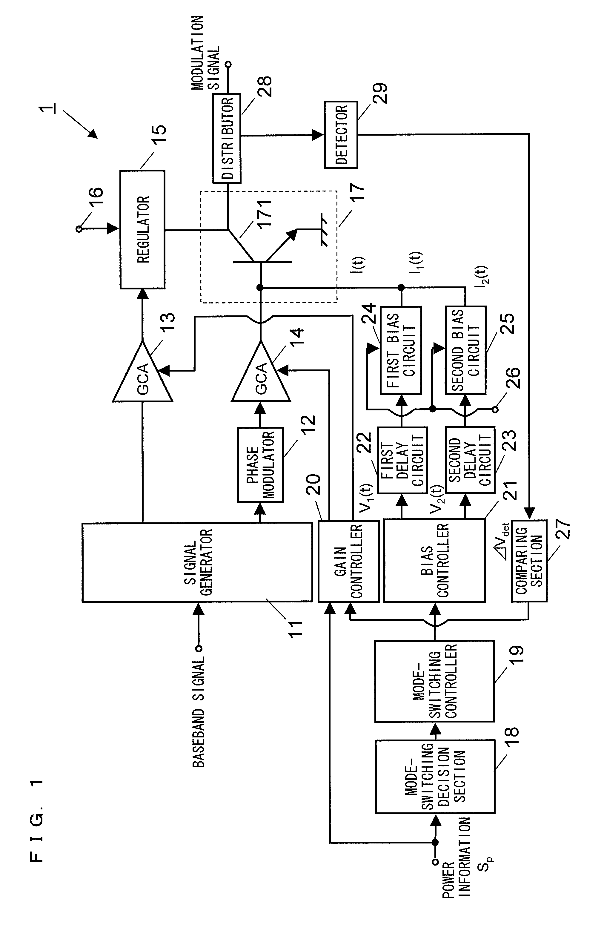
[0042]FIG. 1 is a block diagram showing one configuration example of a transmission circuit 1 according to a first embodiment of the present invention. The transmission circuit 1 in FIG. 1 includes: a signal generator 11; a phase modulator 12; a first variable gain amplifier (GCA) 13; a second variable gain amplifier (GCA) 14; a regulator 15; a power supply terminal 16; a power amplifier 17; a mode-switching decision section 18; a mode-switching controller 19; a gain controller 20; a bias controller 21; a first delay circuit 22; a second delay circuit 23; a first bias circuit 24; a second bias circuit 25; a power supply terminal 26; a comparing section 27; a distributor 28; and a detector 29. The power amplifier 17 includes a transistor for amplification 171.

[0043]In the transmission circuit 1, the signal generator 11 conducts a predefined signal processing on a baseband signal, and generates an amplitude signal and a phase signal. The amplitude signal is inputted into the regulator...

second embodiment

[0077]FIG. 5 is a block diagram showing one configuration example of a transmission circuit 2 according to a second embodiment of the present invention. The transmission circuit 2 in FIG. 5 includes: the signal generator 11; the phase modulator 12; the first variable gain amplifier (GCA) 13; the second variable gain amplifier (GCA) 14; the regulator 15; the power supply terminal 16; the power amplifier 17; a mode-switching decision section 58; a mode-switching controller 59; a gain controller 60; the bias controller 21; the first delay circuit 22; the second delay circuit 23; the first bias circuit 24; the second bias circuit 25; the power supply terminal 26; a comparing section 67; the distributor 28; and a detector 69. The power amplifier 17 includes the transistor for amplification 171.

[0078]When compared to the transmission circuit 1 according to the first embodiment, the characteristic of the transmission circuit 2 according to the second embodiment is conducting the operation ...

third embodiment

[0097]FIG. 9 is a block diagram showing one configuration example of a communication device according to a third embodiment of the present invention. The communication device 200 according to the third embodiment in FIG. 9 includes: a transmission circuit 210; a reception circuit 220; an antenna duplexer 230; and an antenna 240. The transmission circuit 210 is the transmission circuit described above in either the first or the second embodiment. The antenna duplexer 230 transmits a transmission signal outputted from the transmission circuit 210 to the antenna 240, and prevents the transmission signal from leaking into the reception circuit 220. Furthermore, the antenna duplexer 230 transmits a reception signal inputted from the antenna 240 to the reception circuit 220, and prevents the reception signal from leaking into the transmission circuit 210. As a result, the transmission signal is outputted from the transmission circuit 210 and released out into open space from the antenna 2...


PUM


Abstract

A transmission circuit switches a bias circuit without allowing a power amplifier to enter a non-bias state. A first bias circuit supplies a first bias signal to a power amplifier, and a second bias circuit supplies a second bias signal to the power amplifier. A first delay circuit delays the switching of an operation of the first bias circuit using a first delay time, and a second delay circuit delays the switching of an operation of the second bias circuit using a second delay time. The first bias circuit and the second bias circuit are both simultaneously operated for a predefined time period, in order to prevent a transistor for amplification from entering a non-bias state when switching an operation mode of the power amplifier.

Description

BACKGROUND OF THE INVENTION[0001]1. Field of the Invention[0002]The present invention relates to a transmission circuit that is utilized in a communication device such as a mobile phone, a wireless LAN, and the like. More specifically, the present invention relates to a transmission circuit that conducts bias control of a power amplifier.[0003]2. Description of the Background Art[0004]In recent years, in a highly information-oriented society, a communication device such as a mobile phone, a wireless LAN, and the like, have to ensure a linear transmission signal in a broad power amplification range while achieving low power consumption. Adopted in such communication device is a transmission circuit which outputs a transmission signal with high precision regardless of the operation bandwidth and which operates with high efficiency. A conventional transmission circuit is described in the following.[0005]As a conventional transmission circuit, for example, there has been a transmission ...

Claims


Application Information

Patent Timeline
Patent Type & Authority Patents(United States)
IPC IPC(8): H03C3/00H04L27/12H03K7/06
CPCH03F1/0261H03F3/189H03F3/24H03G3/3042H04L27/20H03F2200/105H03F2200/222H03F2200/27H03F2200/387H03F2200/451H03F2200/78
Inventor KITAMURA, RYOISHIDA, KAORU
Owner PANASONIC CORP
Learn More