

Method of Adaptively Selecting Chips for Reducing In-line Testing in a Semiconductor Manufacturing Line
- Summary
- Abstract
- Description
- Claims
- Application Information
AI Technical Summary
Benefits of technology
Problems solved by technology
Method used
Image

Examples
Embodiment Construction
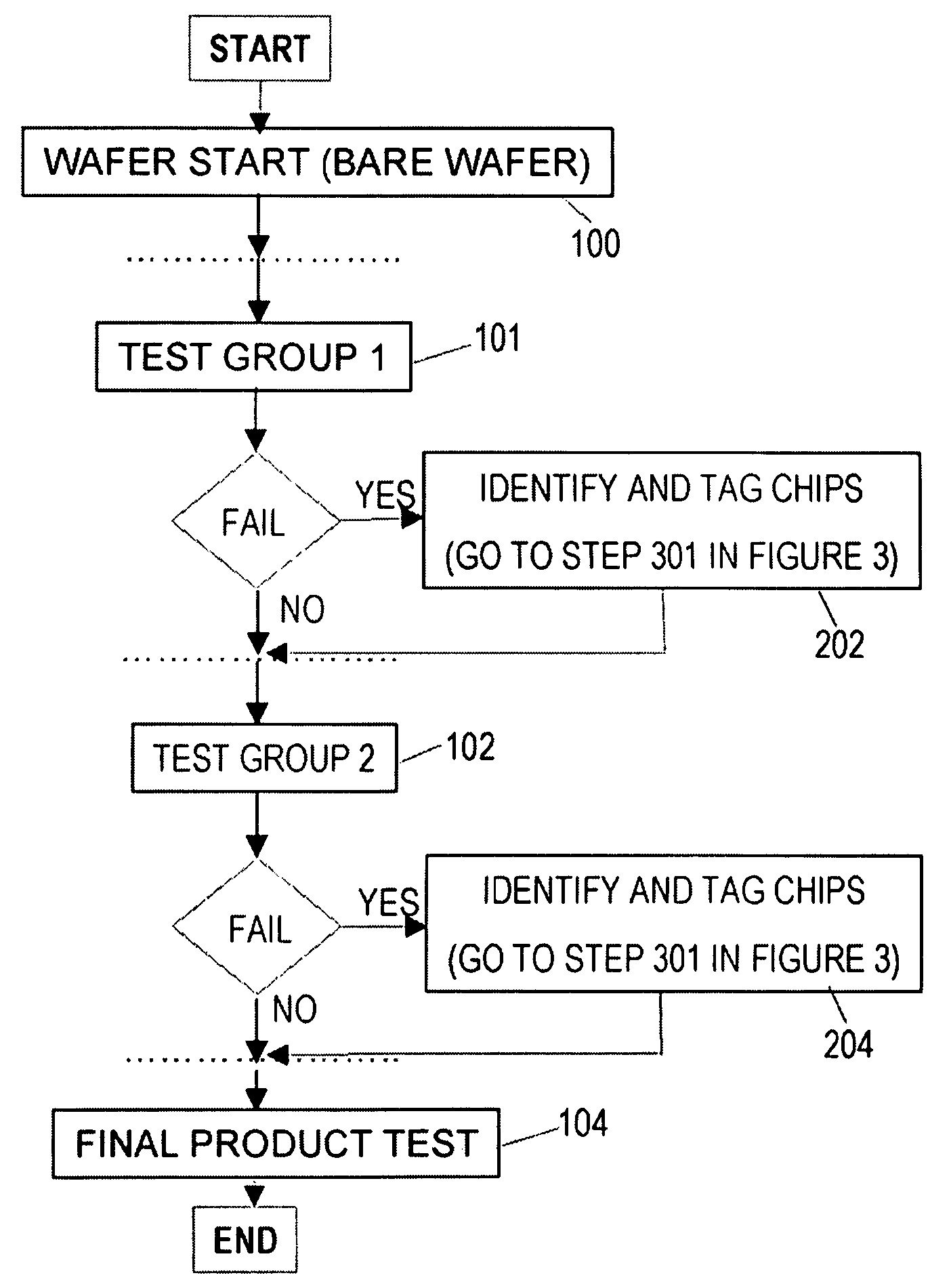
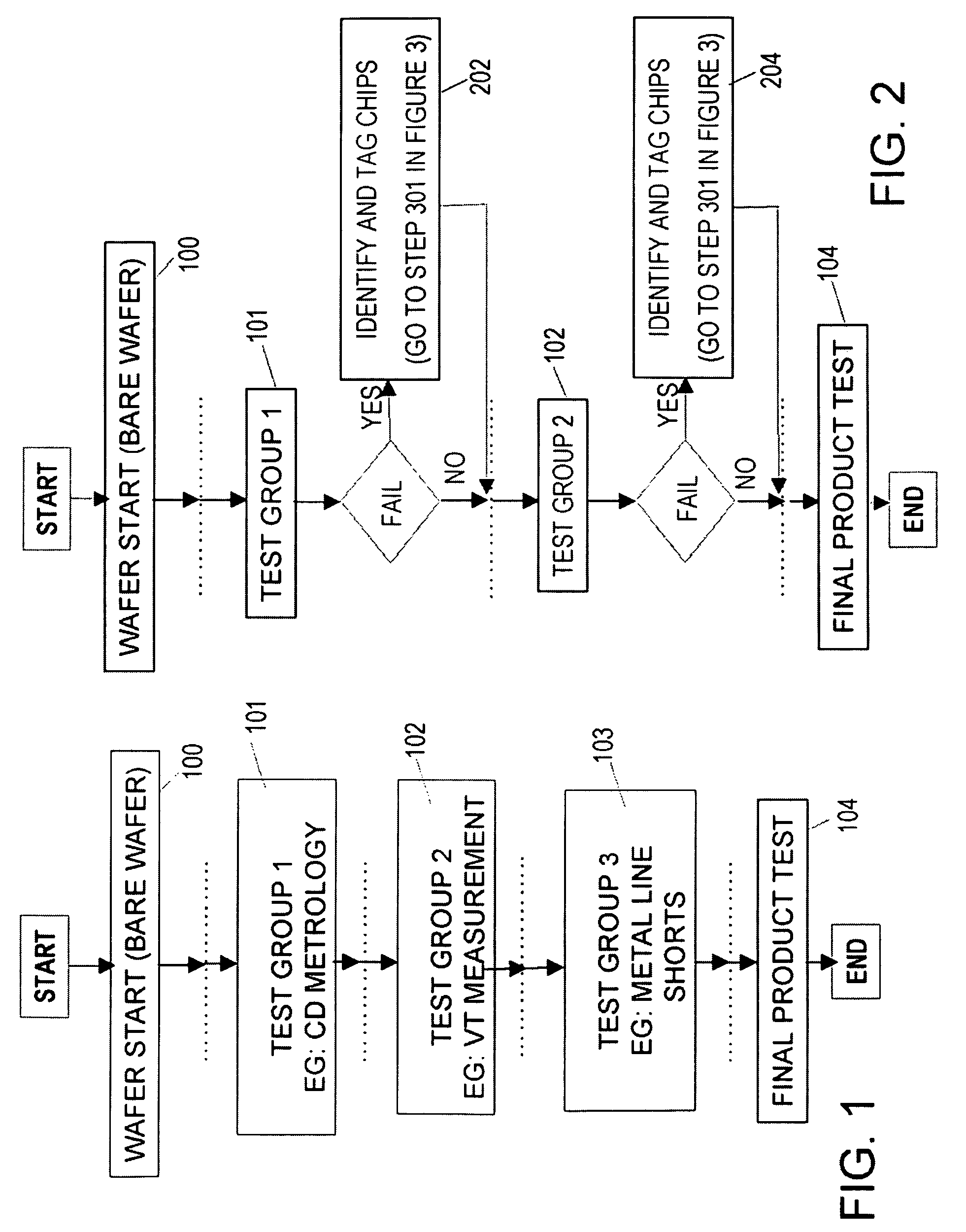
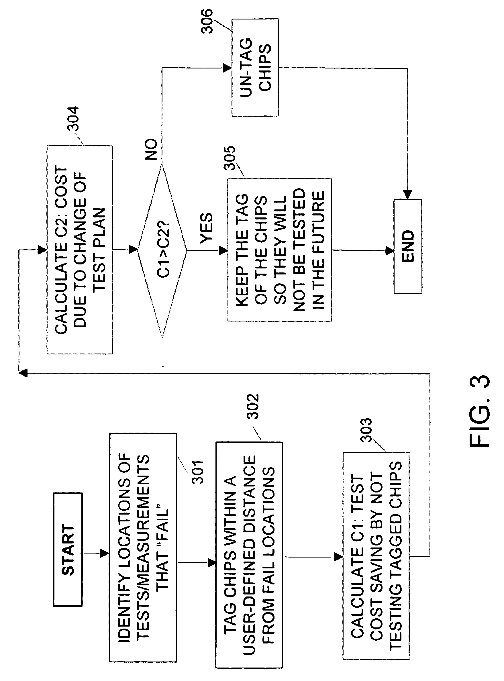
[0009]Accordingly, it is an object of the present invention to provide a system and a method for identifying defective chips early in a manufacturing process, bypassing testing potentially bad chips identified by their respective history of failing certain tests, and allowing only good chips to be further tested.
[0010]It is another object to limit further testing and measurements by taking into consideration the test history of, e.g., in-line tests and measurements during defect inspection (PLY), metrology, parametric, functional tests, wherein the health of a wafer is monitored as it move down a fabrication line.
[0011]It is still another object to reduce the testing time allocated to a wafer by disposing of the wafers or chips that inevitably are misprocessed or affected by defects as they move down a fabrication line.
[0012]It is a further object to provide a system and method that targets potentially bad chips that are excluded from further testing, and that selectively alters the...
PUM
 Abstract
Description
Claims
Application Information