
Resistance ram device having a carbon nano-tube and method for manufacturing the same

a technology of resistance ram and carbon nanotube, which is applied in the field of memory devices, can solve the problems of difficult to obtain a high integration level of a dram, source voltage, and relatively high operation voltage, and achieve the effects of reducing reset current, enhancing sensing margin, and enhancing reliability

Inactive Publication Date: 2009-12-10
SK HYNIX INC
View PDF5 Cites 8 Cited by
  • Summary
  • Abstract
  • Description
  • Claims
  • Application Information

AI Technical Summary

Benefits of technology

[0012]Embodiments of the present invention are also directed to a resistance RAM device capable of enhancing a sensing margin and enhancing the reliability by reducing the reset current and by improving set resistance distribution and reset resistance distribution, and a method for manufacturing the same.

Problems solved by technology

As a result, it is difficult to obtain a high integration level for a DRAM because the surface area of an electrode must be increased.
Further, in flash memory devices, relatively high operation voltages are required as compared to source voltages due to the fact that two gates are stacked on each other.
Accordingly, it is difficult to accomplish a high integration level in a flash memory device because a separate booster circuit is needed to form the necessary voltage for write and delete operations.
However, conventional ReRAM devices exhibit a number of critical problems in that the variation in distribution of set / reset voltages (Vset / Vreset) applied to the binary oxide layer is large and that the distribution of set / reset resistances (Rset / Rreset) is also irregular.

Method used


Image

  • Resistance ram device having a carbon nano-tube and method for manufacturing the same
  • Resistance ram device having a carbon nano-tube and method for manufacturing the same
  • Resistance ram device having a carbon nano-tube and method for manufacturing the same

Examples


Embodiment Construction

[0043]Hereinafter, preferred embodiments of the present invention will be described in detail with reference with accompanying drawings.

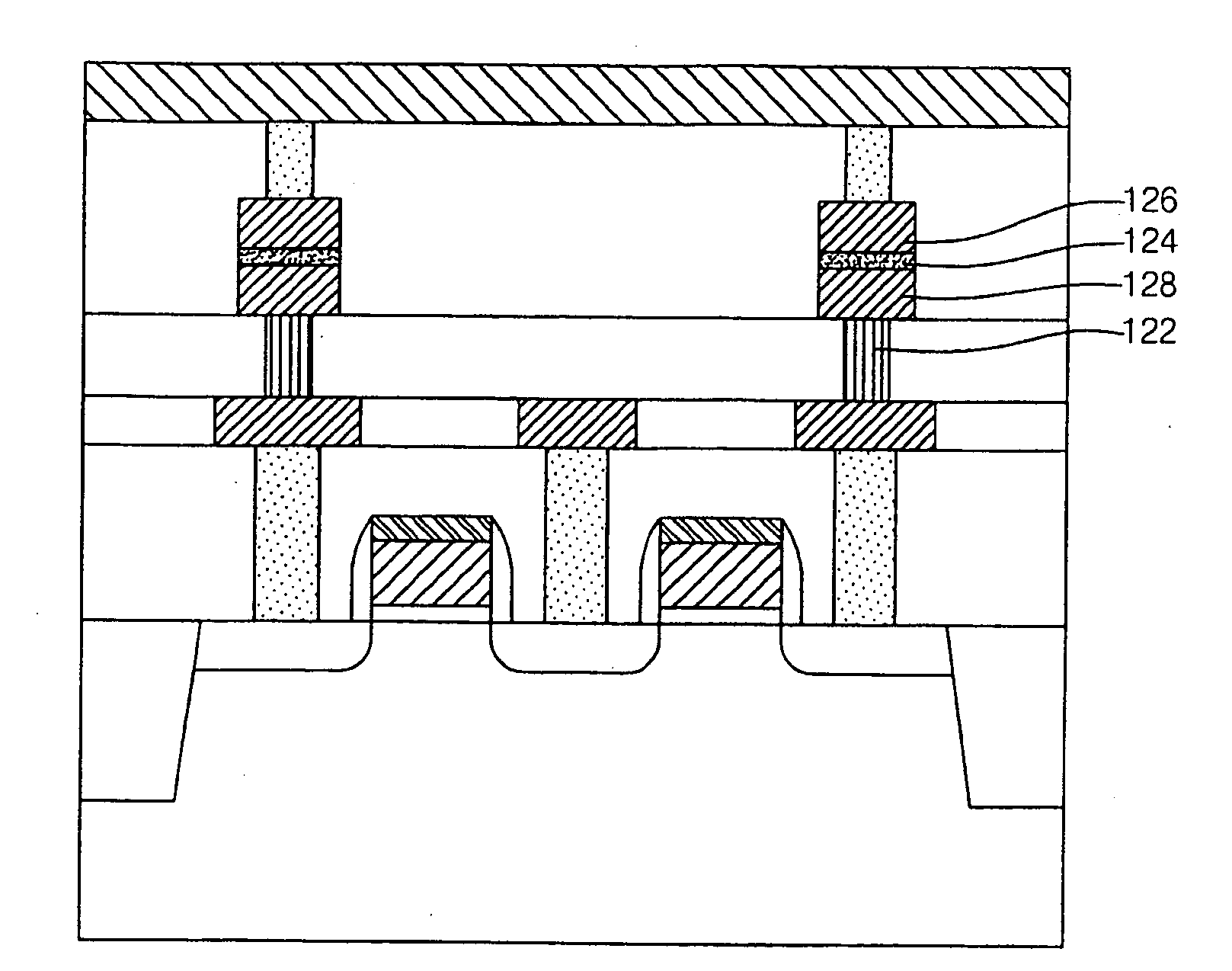
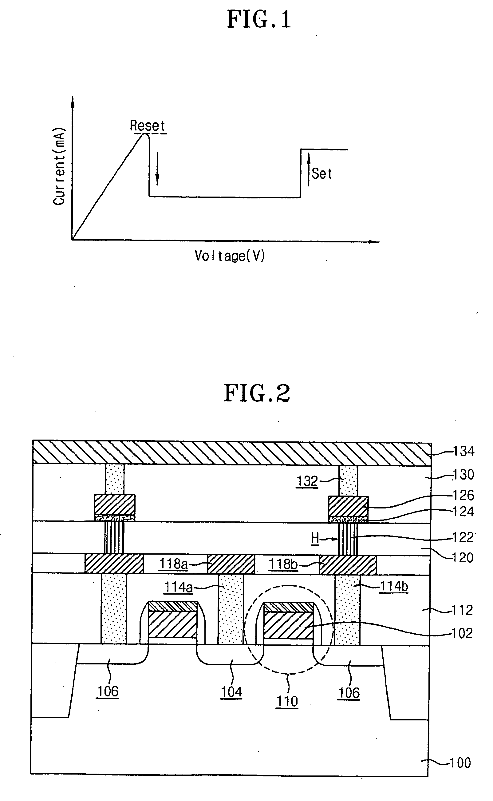
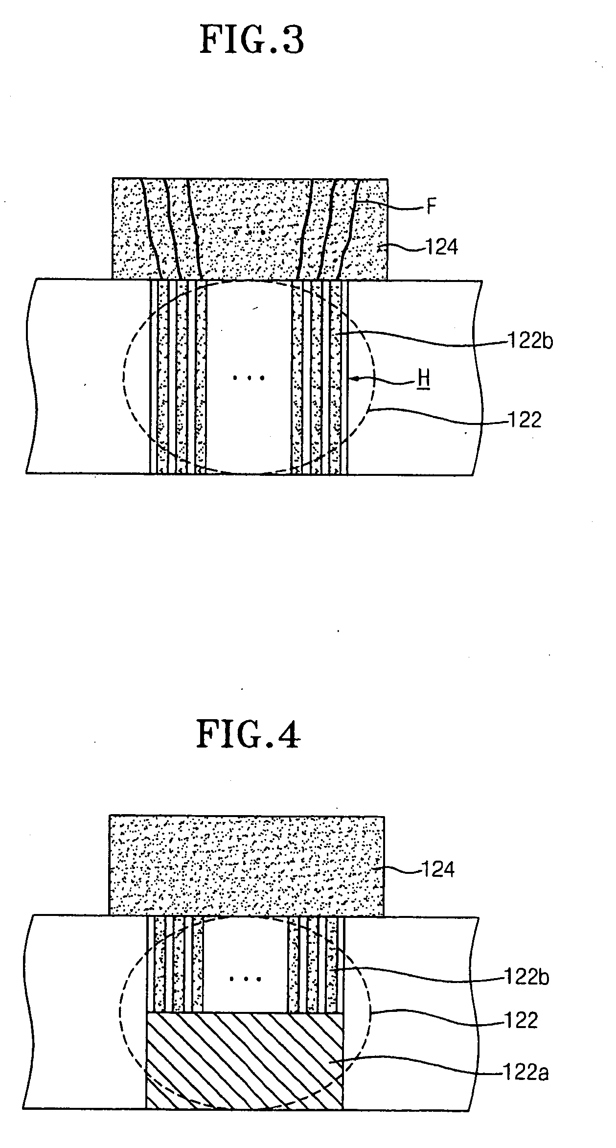
[0044]FIG. 2 is a cross-sectional view illustrating a resistance RAM device in accordance with an embodiment of the present invention. As shown, the resistance RAM device in accordance with an embodiment of the present invention includes a switching device 110 comprised of a transistor, a lower electrode contact 122 electrically connected with the switching device 110 and a binary oxide layer 124 formed over the lower electrode contact 122. The switching device 110 formed of a transistor structure includes a gate area 102, a source area 104 and a drain area. The lower electrode contact 122 is formed by vertically growing at least one carbon nano-tube within a hole H formed so as to expose a metal pad 118b. The binary oxide layer 124 may be formed of any one of NiO, TiO2, ZnO2, ZrO2, Nb2O5, Al2O3 and Ta2O5, and has a dopant that may be formed of any ...


PUM


Abstract

A resistance RAM (ReRAM) device and method of manufacturing the same are presented. The ReRAM exhibits an improved set resistance distribution and an improved reset resistance distribution. The ReRAM device includes a lower electrode contact that has at least one carbon nano-tube; and a binary oxide layer formed over the lower electrode contact. The binary oxide layer is for storing information in accordance to two different resistance states of the binary oxide layer.

Description

CROSS-REFERENCE TO RELATED APPLICATIONS[0001]The present application claims priority to Korean patent application number 10-2008-0052888 filed on Jun. 5, 2008, which is incorporated herein by reference in its entirety.BACKGROUND OF THE INVENTION[0002]The present invention relates to a memory device, more particularly, to a resistance RAM device having an improved Set resistance distribution and a Reset resistance distribution, along with a method for manufacturing the same.[0003]In general, memory devices are largely divided between volatile RAM (random access memory) that loses stored information when power is interrupted and non-volatile ROM (read-only memory) that can continuously maintain the stored state of information even when power is interrupted. RAM devices include DRAM (dynamic RAM) and SRAM (static RAM), whereas ROM devices include flash memory such as an EEPROM (electrically erasable and programmable ROM).[0004]It is well known in the art, that although the DRAM is an e...

Claims


Application Information

Patent Timeline
IPC IPC(8): H01L45/00H01L21/28
CPCH01L27/2436H01L27/2463H01L45/04H01L45/1675H01L45/1273H01L45/146H01L45/1233H10B63/30H10B63/80H10N70/20H10N70/826H10N70/8418H10N70/8833H10N70/011H10N70/063B82Y10/00B82Y40/00H10N70/041
Inventor HWANG, YUN TAEK
Owner SK HYNIX INC
Learn More