
Image Display Device

a display device and image technology, applied in the direction of static indicating devices, instruments, etc., can solve the problems of not ensuring precise correction and creating brightness differences between adjacent pixels

Inactive Publication Date: 2009-12-10
JAPAN DISPLAY INC +1
View PDF9 Cites 29 Cited by
  • Summary
  • Abstract
  • Description
  • Claims
  • Application Information

AI Technical Summary

Benefits of technology

[0016]The present invention has been made in view of the above-mentioned problems of prior art, and it is therefore an object of the present invention to provide a technology with which deterioration of a self-light-emitting element in an image display device can be corrected precisely.

Problems solved by technology

A part in which the white square is displayed deteriorates more quickly than a part in which black is displayed, thereby creating a difference in brightness between adjacent pixels.
The technologies described in JP 2005-156697 A and JP 2002-341825 A therefore do not ensure precise correction even when accurate detection operation is carried out.

Method used


Image

  • Image Display Device
  • Image Display Device
  • Image Display Device

Examples


first embodiment

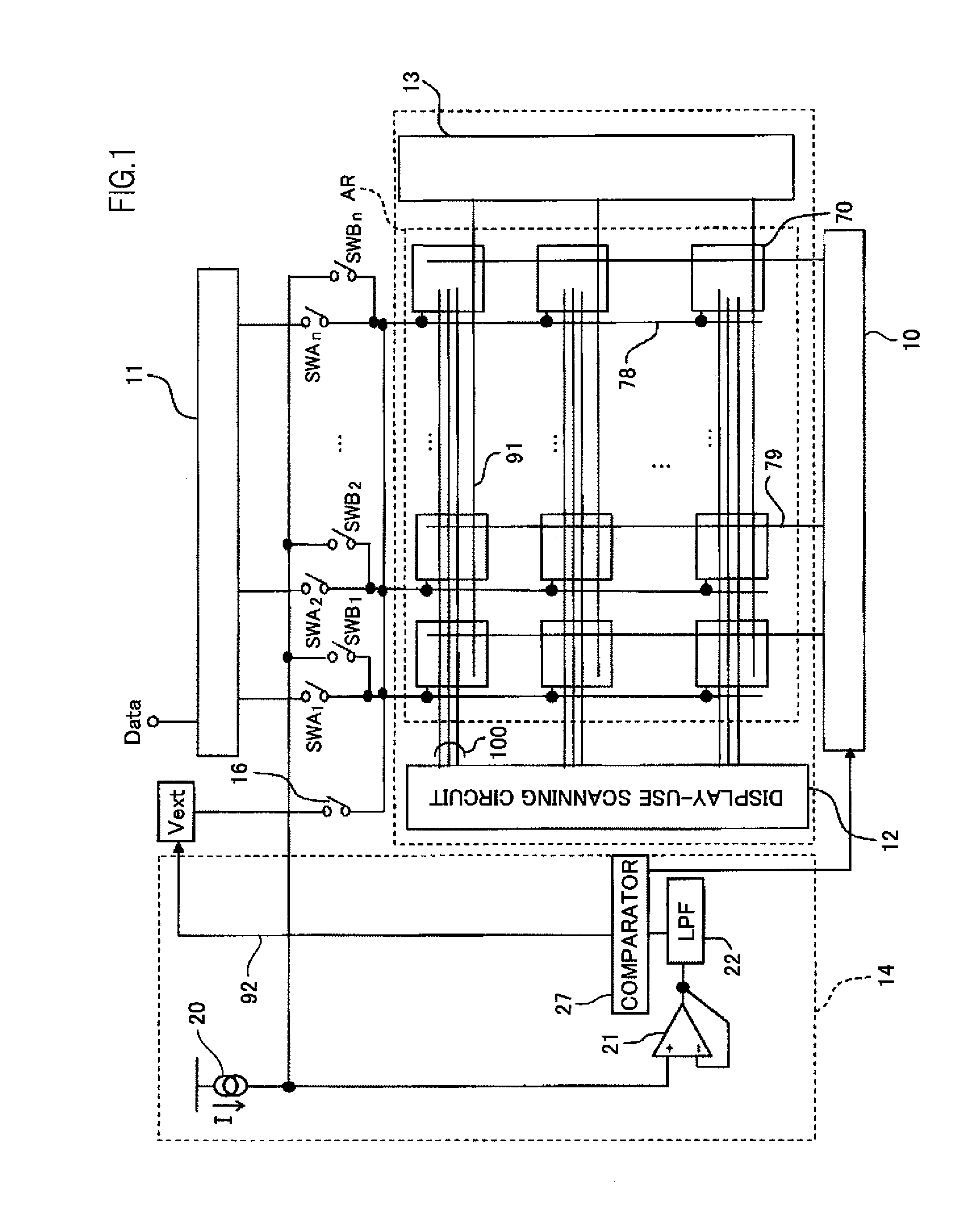
[0046]FIG. 1 is a diagram illustrating a schematic structure of an organic EL display panel with a built-in burn-in detection and correction function according to a first embodiment of the present invention.

[0047]In this embodiment, as illustrated in FIG. 1, a characteristics detection unit 14 first causes a constant current to flow from a current source 20 into each organic EL element, and detects the resultant anode voltage of the organic EL element through a buffer circuit 21 and a low pass filter 22. A comparator 27 compares the detected anode voltage against a threshold voltage.

[0048]When the detected voltage is found to exceed the threshold voltage, one of a reference voltage Vref and a power supply voltage Vdd, which are applied as voltages common to all display pixels, is controlled to prevent burn-in.

[0049]In FIG. 1, denoted by reference symbol “10” is a power supply circuit; “12”, display-use scanning circuit; “13”, detection-use scanning circuit; “16”, external voltage co...

second embodiment

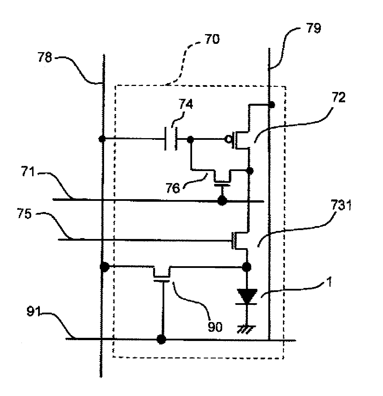
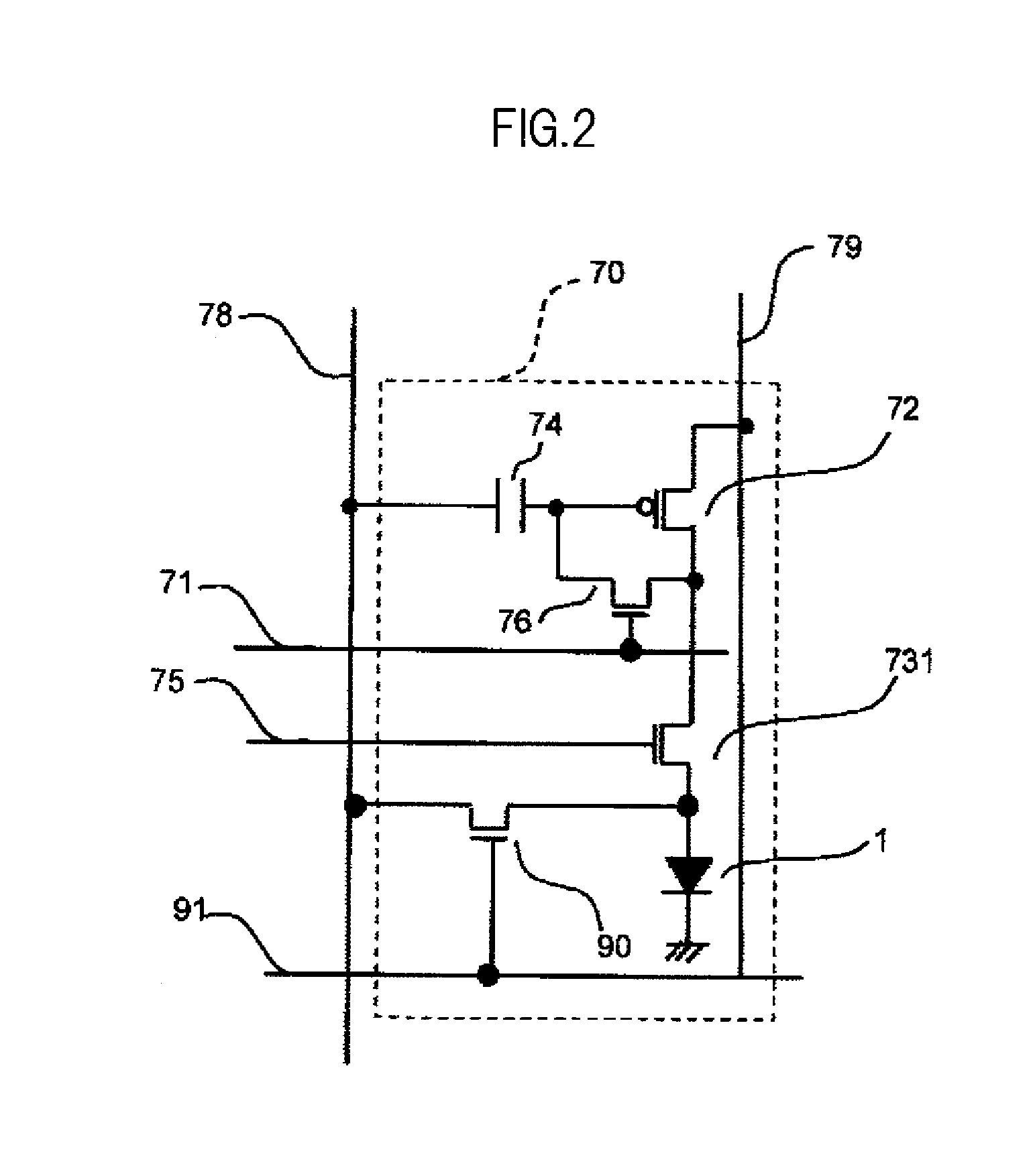
[0092]As can be understood from Expression (2), when the gate length L of the driver TFT 72 is not long enough and the Early voltage 1 / λ is not large enough (i.e., λ is not small enough), a brightness difference of 1% is caused in the current driving method and a correction has to be made for each display pixel. Further, under some conditions, there may be display pixels that cannot secure as the source-drain voltage Vds of the driver TFT 72 a voltage equal to or higher than the overdrive voltage Vref−Vdata and, consequently, cannot employ the current driving method. Accurate correction is impossible in this case because the magnitude of the image voltage to be corrected is varied.

[0093]This embodiment provides a solution by enabling all the display pixels to employ the current driving method and then making a normal correction for each display pixel. Enabling all the display pixels to employ the current driving method is accomplished by controlling one of the following voltages (a)...


PUM


Abstract

Provided is an image display device in which deterioration of a self-light-emitting element within a pixel is corrected accurately. A driver transistor provided in each pixel to drive the self-light-emitting element is driven in a saturation region. A voltage detection unit detects a voltage across the self-light-emitting element of each pixel, which is observed when a constant current is supplied to the self-light-emitting element. When the voltage detected by the voltage detection unit exceeds a threshold voltage, one of a reference voltage and a power supply voltage is controlled to keep an operation region of the driver transistor to the saturation region in every one of a plurality of the pixels of the image display device.

Description

CROSS-REFERENCE TO RELATED APPLICATION[0001]The present application claims priority from Japanese application JP 2008-147016 filed on Jun. 4, 2008, the content of which is hereby incorporated by reference into this application.BACKGROUND OF THE INVENTION[0002]1. Field of the Invention[0003]The present invention relates to an image display device, and more particularly, to an active matrix organic electroluminescence display.[0004]2. Description of the Related Art[0005]There are great expectations on organic electroluminescence displays (hereinafter referred to as organic EL display devices) which each include an organic electroluminescence display panel (hereinafter referred to as organic EL display panel) driven by active matrix driving, as flat panel displays of a next generation.[0006]The organic EL display panel usually includes an organic electroluminescence element (hereinafter referred to as organic EL element) and a driving-use thin film transistor for supplying a current to...

Claims


Application Information

Patent Timeline
Patent Type & Authority Applications(United States)
IPC IPC(8): G09G3/30
CPCG09G3/3233G09G3/3275G09G2300/043G09G2320/046G09G2300/0819G09G2320/045G09G2300/0814
Inventor KOHNO, TOHRUAKIMOTO, HAJIMEKASAI, NARUHIKOISHII, MASATO
Owner JAPAN DISPLAY INC
Features
  • Generate Ideas
  • Intellectual Property
  • Life Sciences
  • Materials
  • Tech Scout
  • Unparalleled Data Quality
  • Higher Quality Content
  • 60% Fewer Hallucinations
Learn More