High Resistivity Metal Fan Out

a metal fan and high resistivity technology, applied in the direction of dielectric characteristics, programmable/customizable/modifiable circuits, instruments, etc., can solve the problems of wider, thicker traces are generally of higher reliability, etc., to improve reliability, improve noise rejection, and reduce manufacturing costs

Active Publication Date: 2009-12-10
APPLE INC
View PDF37 Cites 66 Cited by
  • Summary
  • Abstract
  • Description
  • Claims
  • Application Information

AI Technical Summary

Benefits of technology

[0004]This relates to the formation of metal traces in the border areas of a touch sensor panel to provide improved reliability, better noise rejection, and lower manufacturing costs. The metal traces can be coupled to rows on the touch sensor panel in an interleaved manner, so that any two successive rows can be coupled to metal traces in border areas on opposite sides of the touch sensor panel. In addition, by utilizing the full width available in the border areas in some embodiments, the metal traces can be formed from higher resistivity metal, which can reduce manufacturing costs and improve trace reliability. The wider traces can also provide better noise immunity from noise sources such as an LCD by providing a larger fixed-potential surface area and by more effectively coupling the drive lines to the fixed potential.
[0005]By making the metal traces fill up the available width of the border areas, the traces can be wider and thus the overall line resistance of the trace can be lower, or the resistivity of the material can be increased for the same overall line resistance. For example, a single thicker and wider layer of Molybdenum / Niobium (Mo / Nb) having a thickness of about 3000-5000 Å can be formed on a substrate. The higher resistivity of Mo / Nb is compensated for by the increased width and height of the Mo / Nb layer. After the Mo / Nb layer is deposited at the preferred thickness, it can be patterned (etched) to form traces. A layer of conductive material such as ITO can then be formed over the Mo / Nb layer. A conductive material layer can then be patterned to form the drive or sense lines that couple to the metal traces, and can also be patterned over the Mo / Nb traces to form another protective layer for the Mo / Nb traces. A protective layer of material such as silicon oxide (SiO2) can then be formed over the Mo / Nb layer and the conductive material layer.
[0006]In general, the ability to use higher resistivity material enables more flexibility in the material stack. For example, in two conductive layer embodiments, manufacturing costs can be reduced as compared to three-layer stackups of thin, higher conductivity material. The fewer number of conductive layers also reduces the problem of side wall control present in when multi-layer stackups are patterned. In addition, the wider, thicker traces are generally of higher reliability, because etching defects, corrosion or other environmental effects may not create problems as easily as if the traces were thinner.
[0007]Although the embodiments described above utilize higher resistivity conductive material, such material need not be used. If low resistivity material is used to form the wide traces, the line resistance can be made even lower. This reduced line resistance can produce a better coupling to ground (or some fixed potential) for the wide row traces, improving the noise shielding effectiveness of the rows. Alternatively, a low resistance material can be used with the traces widths kept thin. The thin metal traces can enable a reduction in the width of the touch sensor panel. For example, a thinned three-layer stackup including low resistance material can be used, and in some cases may be less expensive than to develop an alternate chemistry two-layer stackup.

Problems solved by technology

In addition, the wider, thicker traces are generally of higher reliability, because etching defects, corrosion or other environmental effects may not create problems as easily as if the traces were thinner.

Method used


Image

  • High Resistivity Metal Fan Out
  • High Resistivity Metal Fan Out
  • High Resistivity Metal Fan Out

Examples


Embodiment Construction

[0017]In the following description of preferred embodiments, reference is made to the accompanying drawings which form a part hereof, and in which it is shown by way of illustration specific embodiments in which the invention can be practiced. It is to be understood that other embodiments can be used and structural changes can be made without departing from the scope of the embodiments of this invention.

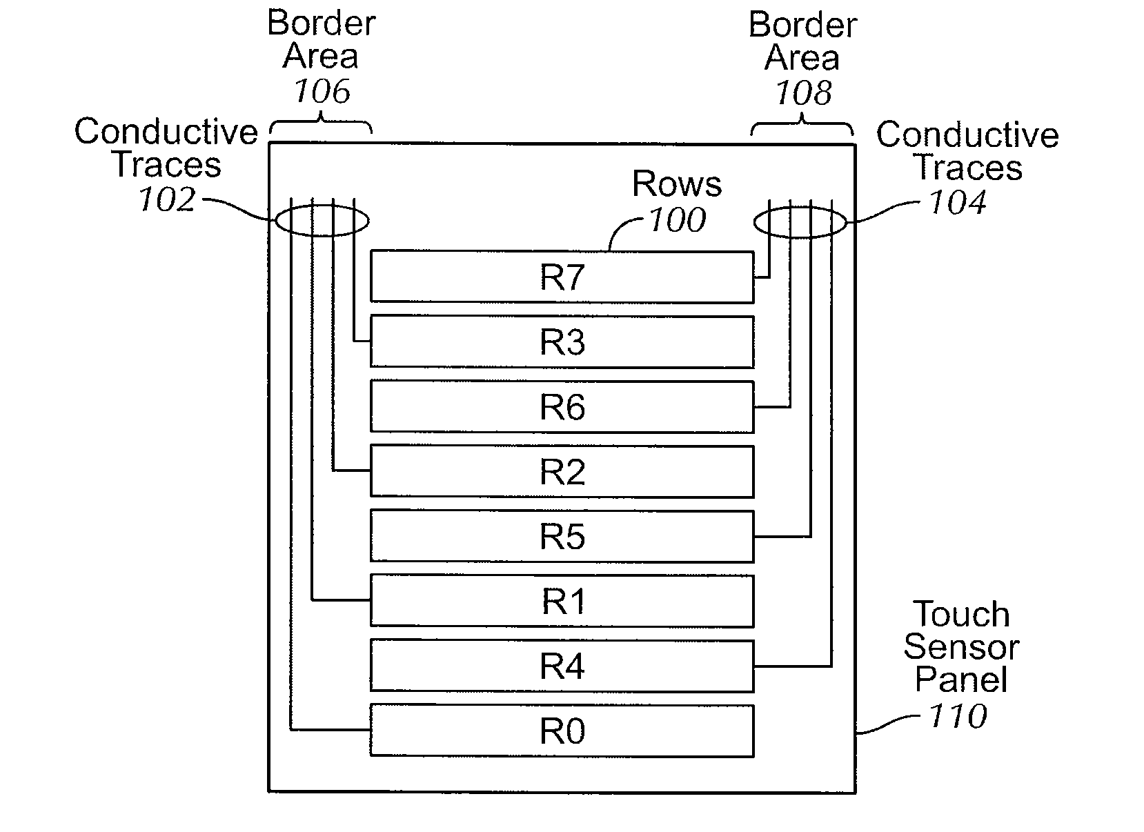
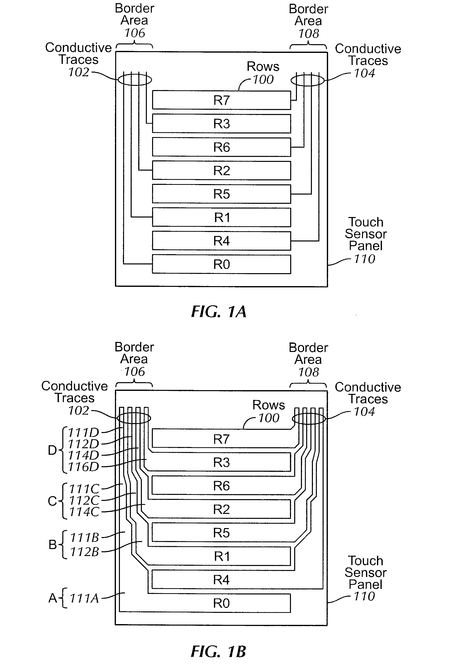
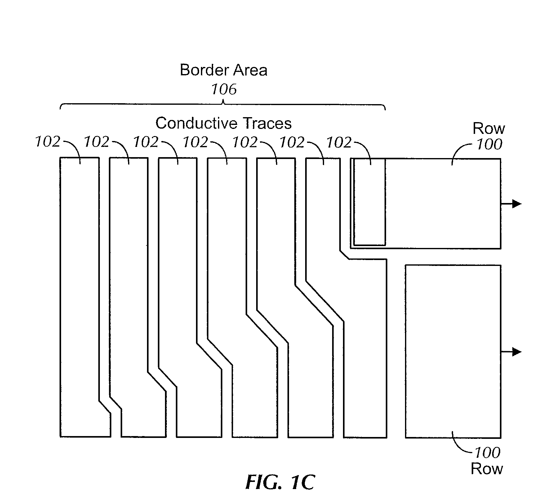
[0018]This relates to the formation of metal traces in the border areas of a touch sensor panel to provide improved reliability, better noise rejection, and lower manufacturing costs. The metal traces can be coupled to rows on the touch sensor panel in an interleaved manner, so that any two successive rows can be coupled to metal traces in border areas on opposite sides of the touch sensor panel. In addition, by utilizing the full width available in the border areas, the metal traces can be formed from higher resistivity metal, which can reduce manufacturing costs and improve trace r...


PUM


Abstract

The formation of metal traces in the border areas of a touch sensor panel to provide improved reliability, better noise rejection, and lower manufacturing costs is disclosed. The metal traces can be coupled to rows on the touch sensor panel in an interleaved manner, so that any two successive rows can be coupled to metal traces in border areas on opposite sides of the touch sensor panel. In addition, by utilizing the full width available in the border areas in some embodiments, the metal traces can be formed from higher resistivity metal, which can reduce manufacturing costs and improve trace reliability. The wider traces can also provide better noise immunity from noise sources such as an LCD by providing a larger fixed-potential surface area and by more effectively coupling the drive lines to the fixed potential.

Description

FIELD OF THE INVENTION [0001]This relates generally to the formation of metal traces on substrates, and more particularly, to the formation of metal traces in the border areas of a touch sensor panel in a manner that allows for higher resistivity conductive materials to be used to improve trace reliability, reduce noise, and lower manufacturing costs.BACKGROUND OF THE INVENTION [0002]Many types of input devices are presently available for performing operations in a computing system, such as buttons or keys, mice, trackballs, joysticks, touch sensor panels, touch screens and the like. Touch screens, in particular, are becoming increasingly popular because of their ease and versatility of operation as well as their declining price. Touch screens can include a touch sensor panel, which can be a clear panel with a touch-sensitive surface, and a display device such as a liquid crystal display (LCD) that can be positioned partially or fully behind the panel so that the touch-sensitive sur...

Claims


Application Information

Patent Timeline
Patent Type & Authority Applications(United States)
IPC IPC(8): G06F3/041
CPCG06F3/044G06F3/0446G06F3/0445H05K3/24H05K2201/0108H05K1/0289G06F2203/04103G06F2203/04107G06F3/0448G06F3/04164G06F3/0412G06F2203/04102G06F2203/04113
Inventor GRUNTHANER, MARTIN PAULHUANG, LILI
Owner APPLE INC
Why Eureka
Try Eureka