Thin silicon single diffusion field effect transistor for enhanced drive performance with stress film liners

a single diffusion field and transistor technology, applied in the field of thin silicon single diffusion field effect transistors for enhanced drive performance with stress film liners, integrated semiconductor devices, etc., can solve problems such as unknown prior ar

Inactive Publication Date: 2009-12-10
IBM CORP
View PDF100 Cites 11 Cited by
  • Summary
  • Abstract
  • Description
  • Claims
  • Application Information

AI Technical Summary

Benefits of technology

[0012]An even further object of the present invention is to reduce the offset spacer dimension to below 3 nm or to eliminate them completely, maximizing the stress imparted to the channel. In this embodiment of the present invention, the diffusion junction are annealed, i.e., activated, using an advanced annealing technique, such as, a laser anneal, to avoid high levels of dopant diffusion into the channel and to avoid the poor short channel characteristics that would occur.
[0019]In some embodiments, of the present invention, a single diffusion spacer (i.e., offset spacer) is present on the sidewalls of the FET. The single diffusion spacer employed in the present invention is an ultra-thin spacer having a lateral dimension from about 3 to about 20 nm. In some embodiments, the single diffusion spacer can be scaled to below 3 nm or even eliminated when an advanced thermal process is used for activating the single, continuous diffusion regions.
[0029]In some embodiments, of the present invention, a single diffusion spacer (i.e., offset spacer) is formed on the sidewalls of the at least one patterned gate region. The single diffusion spacer employed in the present invention is an ultra-thin spacer having a lateral dimension from about 3 to about 20 nm. In some embodiments, the single diffusion spacer can be scaled to below 3 nm or even eliminated when an advanced thermal process is used for activating the single, continuous diffusion regions.

Problems solved by technology

To date, there is no known prior art that combines the use of a thin SOI layer (having a thickness of about 50 nm or less) with dual stress liners in providing a field effect transistor that has enhanced drive current performance.

Method used


Image

  • Thin silicon single diffusion field effect transistor for enhanced drive performance with stress film liners
  • Thin silicon single diffusion field effect transistor for enhanced drive performance with stress film liners
  • Thin silicon single diffusion field effect transistor for enhanced drive performance with stress film liners

Examples


Embodiment Construction

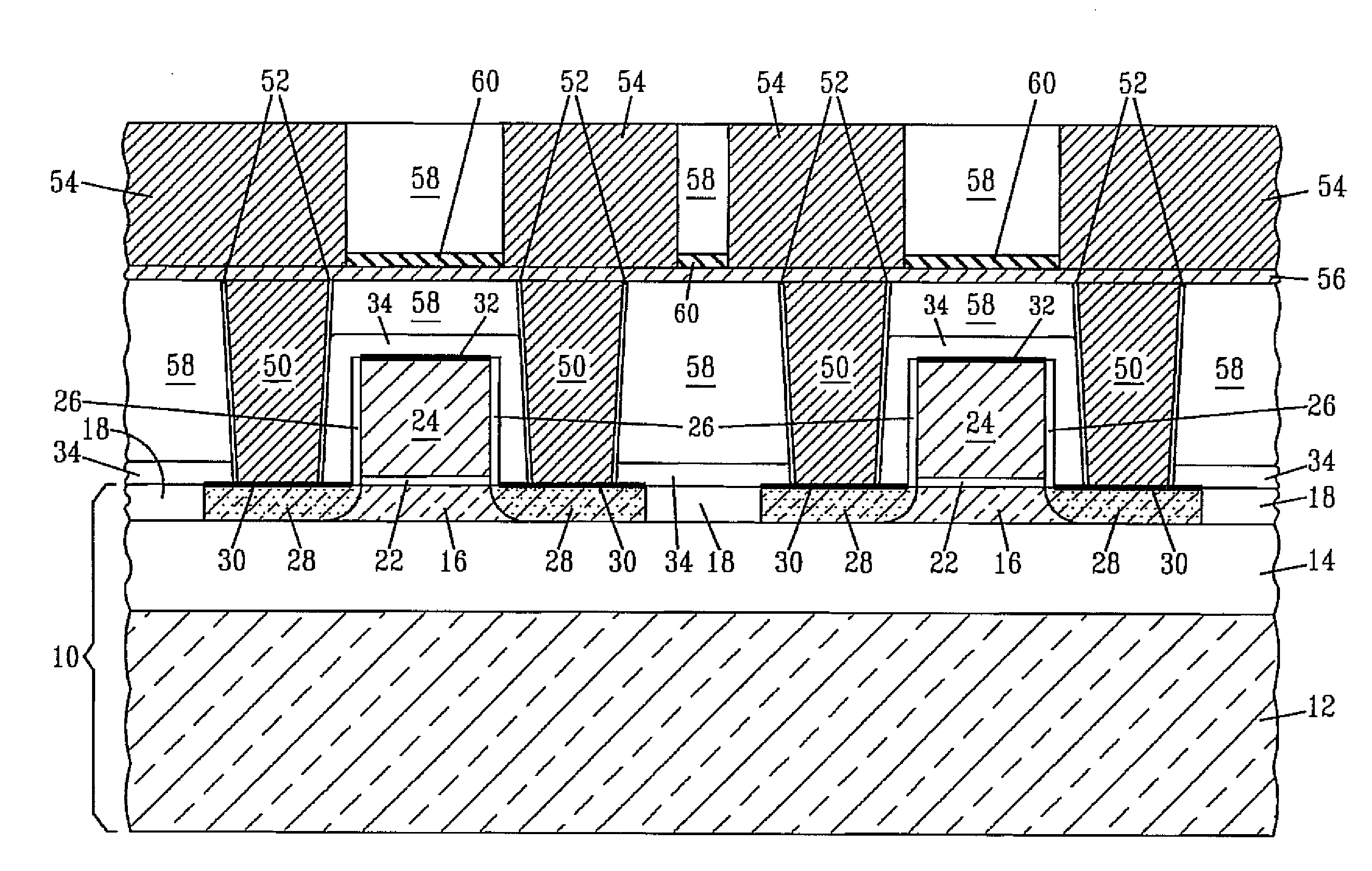
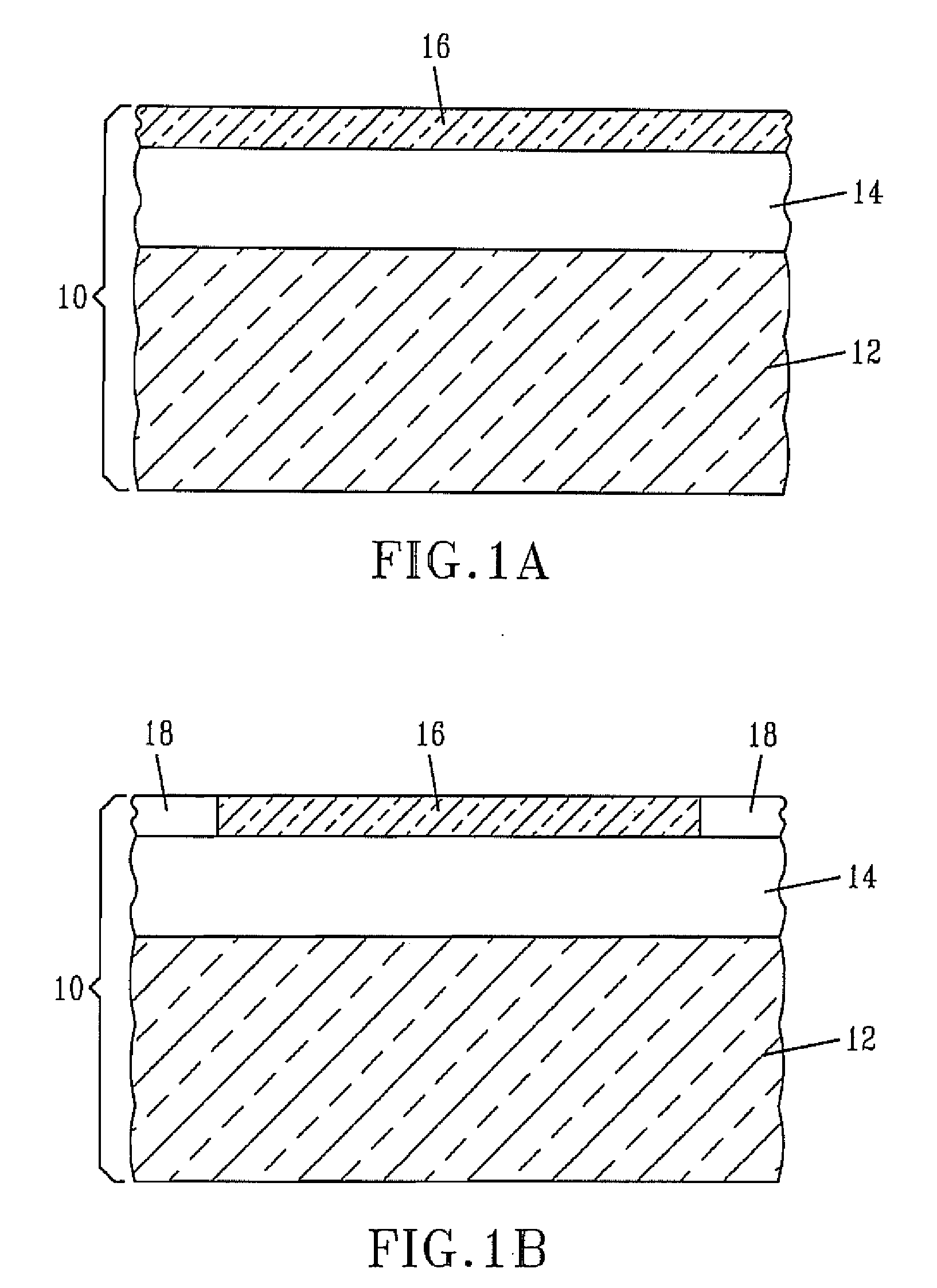
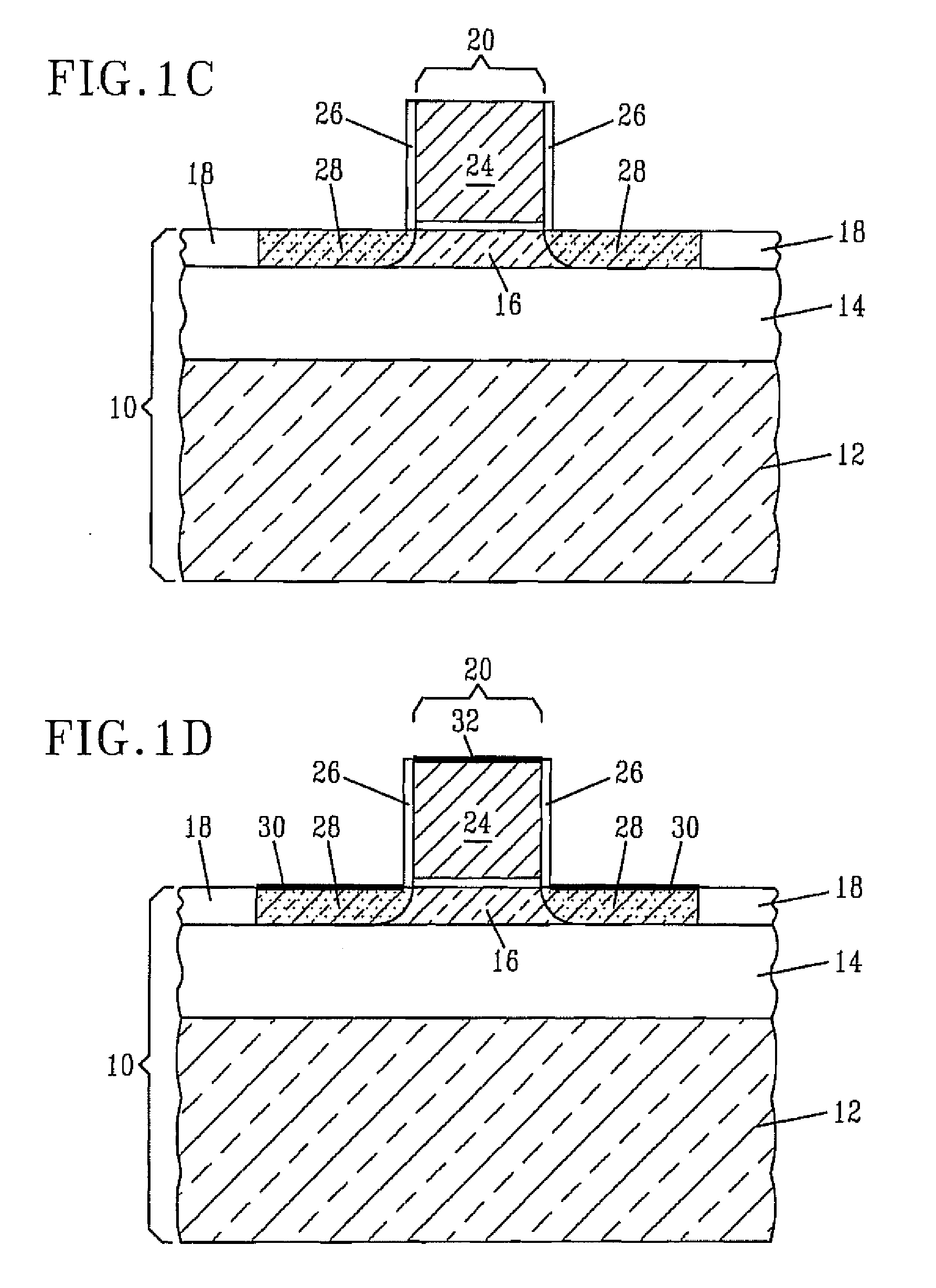
[0033]The present invention, which provides a thin silicon single diffusion FET for enhanced drive current performance with stress liners, will now be described in greater detail by referring to the following discussion as well as the drawings that accompany the present application. In the accompanying drawings, like and correspondence elements are referred to by like reference numerals. It is noted that the drawings of the present application are provided for illustrative purposes and thus they are not drawn to scale.

[0034]The present invention will now be described in detail by first referring to FIGS. 1A-1F which are cross sectional views illustrating the basic processing steps of the present invention. In this embodiment, a single FET device is shown. Although a single FET device is shown and illustrated, the present invention also works equally well when a plurality of FETs are formed. In embodiments in which a plurality of FETs are formed, the FETs may have the same polarity (...


PUM


Abstract

The present invention provides a semiconducting device structure including a thin SOI region, wherein the SOI device is formed with an optional single thin diffusion, i.e., offset, spacer and a single diffusion implant. The device silicon thickness is thin enough to permit the diffusion implants to abut the buried insulator but thick enough to form a contacting silicide. Stress layer liner films are used both over nFET and pFET device regions to enhance performance.

Description

CROSS REFERENCE TO RELATED APPLICATION[0001]This application is a divisional application of U.S. Ser. No. 11 / 329,490 filed on Jan. 11, 2006 entitled “THIN SILICON SINGLE DIFFUSION FIELD EFFECT TRANSISTOR FOR ENHANCED DRIVE PERFORMANCE WITH STRESS FILM LINERS”. The entire content of of the aforementioned U.S. application is incorporated herein.FIELD OF THE INVENTION[0002]The present invention relates to semiconductor devices, and more particularly to integrated semiconductor devices, such as complementary metal oxide semiconductor (CMOS) devices, located atop a substrate having a thin (on the order of about 50 nm or less) semiconductor-on-insulator (SOI) layer. In particular, the present invention forms nFET (field effect transistor) and pFET devices on the thin SOI layer. In additional to being located on a thin SOI layer, the FET devices of the present invention include an optional single ultra-thin diffusion spacer, a single diffusion junction, and dual stress film liners. Dual st...

Claims


Application Information

Patent Timeline
Patent Type & Authority Applications(United States)
IPC IPC(8): H01L21/762H01L21/8238H01L21/336
CPCH01L21/84H01L27/1203H01L29/7843H01L29/66772H01L29/458
Inventor CHANG, LELANDFRIED, DAVID M.HERGENROTHER, JOHN M.SHAHIDI, GHAVAMSLEIGHT, JEFFREY W.
Owner IBM CORP
Why Eureka
Try Eureka