
Thin silicon single diffusion field effect transistor for enhanced drive performance with stress film liners

a single diffusion field and transistor technology, applied in the field of thin silicon single diffusion field effect transistors for enhanced drive performance with stress film liners, integrated semiconductor devices, etc., can solve problems such as unknown prior ar

Inactive Publication Date: 2007-07-12
IBM CORP
View PDF99 Cites 15 Cited by
  • Summary
  • Abstract
  • Description
  • Claims
  • Application Information

AI Technical Summary

Benefits of technology

The present invention provides a semiconductor device that includes a thin SOI layer with a device channel thickness of less than 50 nm and a single diffusion region that is formed by a single ion implantation step. The device also includes a stressed liner that transfers stress to the device channel and a silicide contact can be located in the upper semiconductor layer. The invention also provides a method of fabricating the semiconductor device. The technical effects of the invention include improved performance, reduced contact resistance, and improved reliability of the semiconductor device.

Problems solved by technology

To date, there is no known prior art that combines the use of a thin SOI layer (having a thickness of about 50 nm or less) with dual stress liners in providing a field effect transistor that has enhanced drive current performance.

Method used


Image

  • Thin silicon single diffusion field effect transistor for enhanced drive performance with stress film liners
  • Thin silicon single diffusion field effect transistor for enhanced drive performance with stress film liners
  • Thin silicon single diffusion field effect transistor for enhanced drive performance with stress film liners

Examples


Embodiment Construction

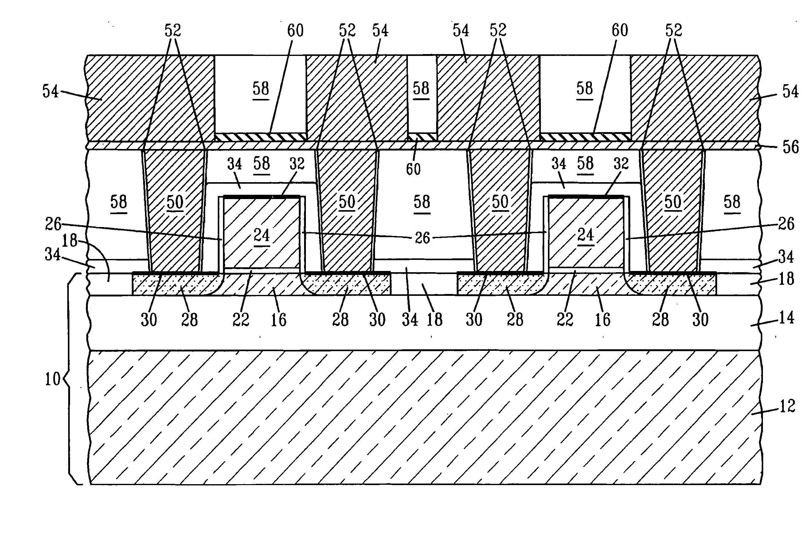
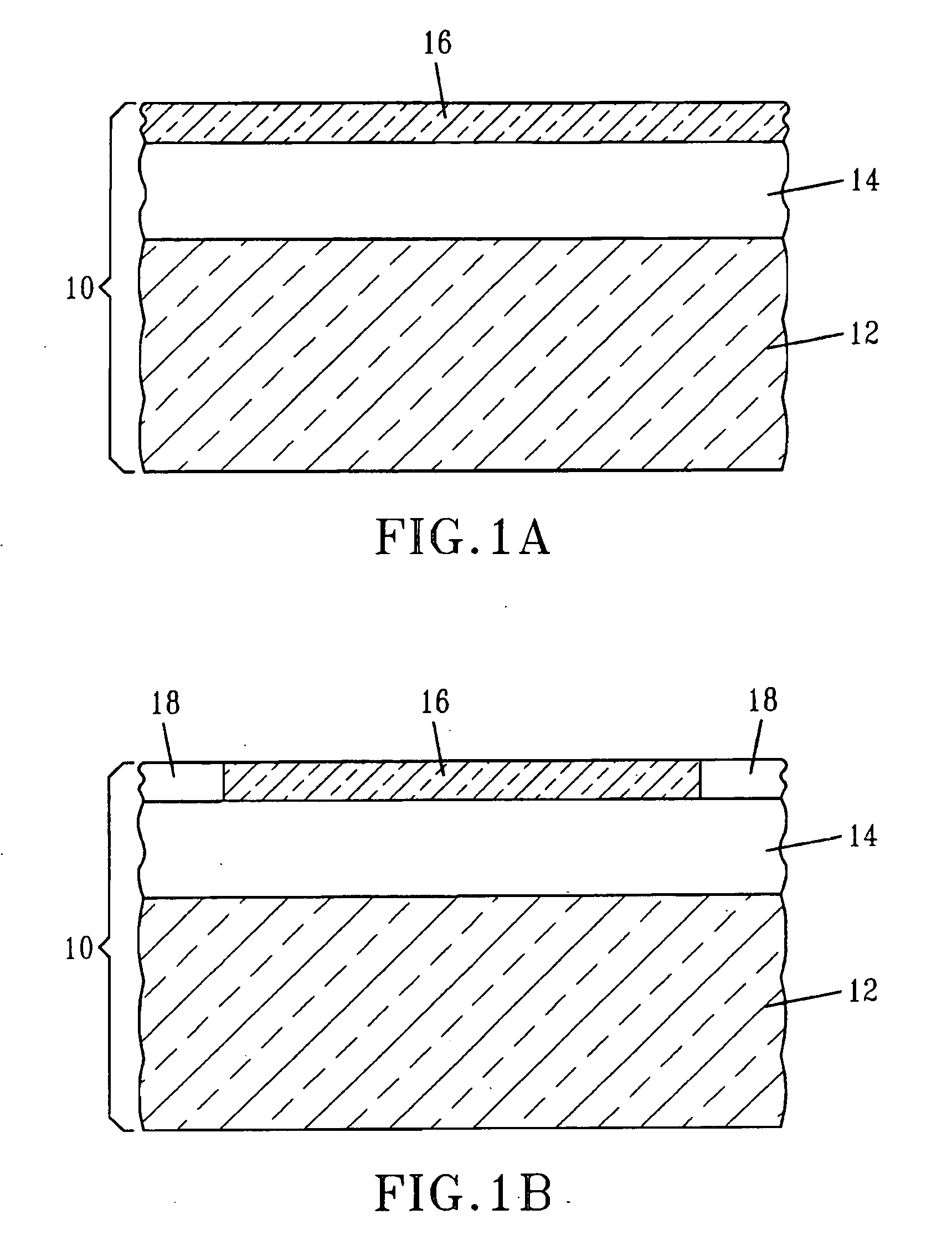
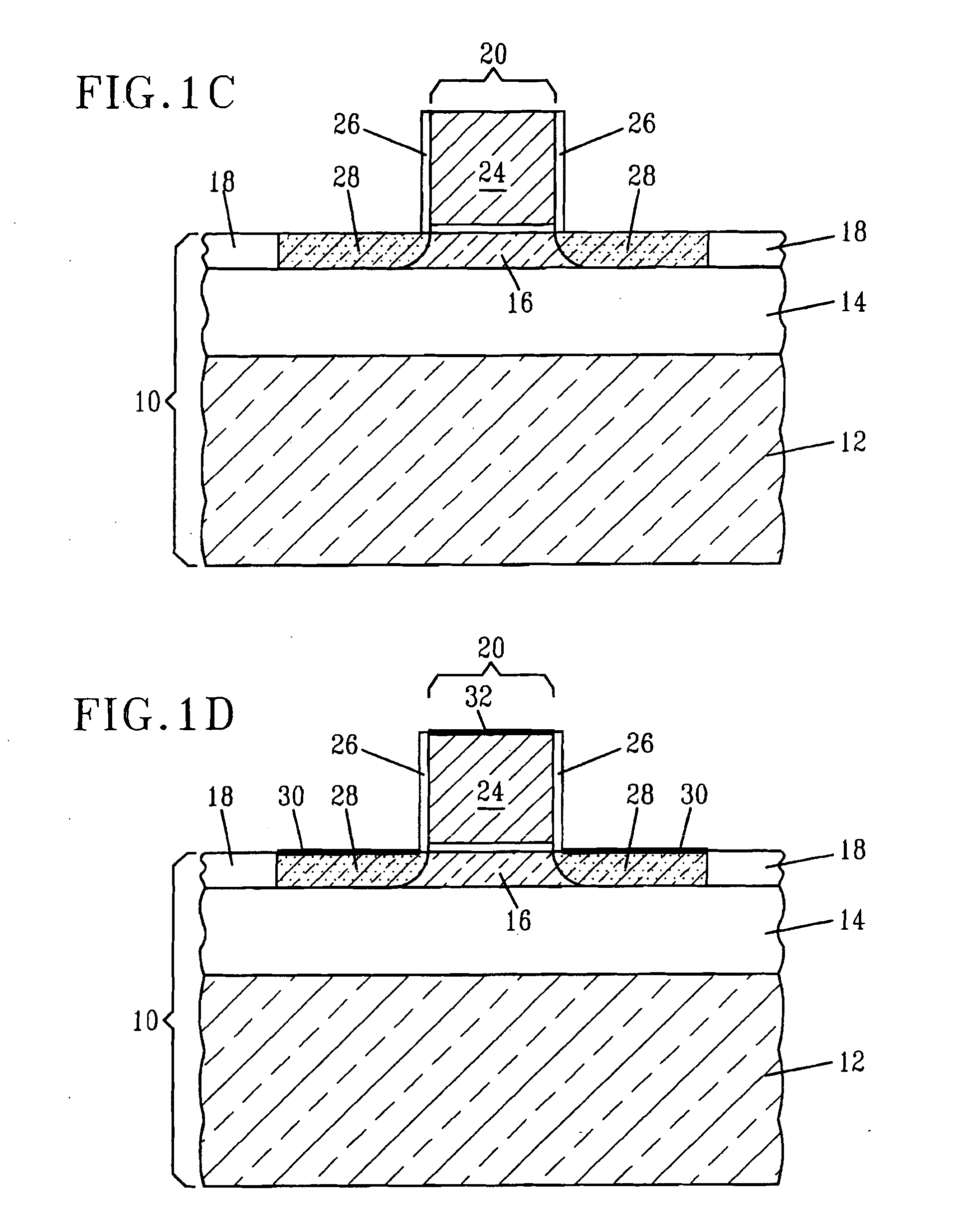
[0032] The present invention, which provides a thin silicon single diffusion FET for enhanced drive current performance with stress liners, will now be described in greater detail by referring to the following discussion as well as the drawings that accompany the present application. In the accompanying drawings, like and correspondence elements are referred to by like reference numerals. It is noted that the drawings of the present application are provided for illustrative purposes and thus they are not drawn to scale.

[0033] The present invention will now be described in detail by first referring to FIGS. 1A-1F which are cross sectional views illustrating the basic processing steps of the present invention. In this embodiment, a single FET device is shown. Although a single FET device is shown and illustrated, the present invention also works equally well when a plurality of FETs are formed. In embodiments in which a plurality of FETs are formed, the FETs may have the same polarit...


PUM


Abstract

The present invention provides a semiconducting device structure including a thin SOI region, wherein the SOI device is formed with an optional single thin diffusion, i.e., offset, spacer and a single diffusion implant. The device silicon thickness is thin enough to permit the diffusion implants to abut the buried insulator but thick enough to form a contacting silicide. Stress layer liner films are used both over nFET and pFET device regions to enhance performance.

Description

FIELD OF THE INVENTION [0001] The present invention relates to semiconductor devices, and more particularly to integrated semiconductor devices, such as complementary metal oxide semiconductor (CMOS) devices, located atop a substrate having a thin (on the order of about 50 nm or less) semiconductor-on-insulator (SOI) layer. In particular, the present invention forms nFET (field effect transistor) and pFET devices on the thin SOI layer. In additional to being located on a thin SOI layer, the FET devices of the present invention include an optional single ultra-thin diffusion spacer, a single diffusion junction, and dual stress film liners. Dual stress film liners have been described previously in the art, and usually incorporate one stress film type (typically tensile) to enhance nFET drive current performance and another stress film type (typically compressive) to enhance pFET drive current performance. BACKGROUND OF THE INVENTION [0002] Semiconductor-on-insulator (SOI) devices, par...

Claims


Application Information

Patent Timeline
Patent Type & Authority Applications(United States)
IPC IPC(8): H01L27/12
CPCH01L21/84H01L27/1203H01L29/7843H01L29/66772H01L29/458
Inventor CHANG, LELANDFRIED, DAVID M.HERGENROTHER, JOHN M.SHAHIDI, GHAVAMSLEIGHT, JEFFREY W.
Owner IBM CORP
Learn More