Method for manufacturing semiconductor memory device

a semiconductor memory and manufacturing method technology, applied in the direction of microlithography exposure apparatus, instruments, photomechanical treatment, etc., can solve the problems of bit line leakage current not meeting the above condition of 5 a, and the leakage current of bit lines may increase, so as to minimize the irregularity of a leakage current in bit lines

Inactive Publication Date: 2009-12-10
DONGBU HITEK CO LTD
View PDF4 Cites 0 Cited by
  • Summary
  • Abstract
  • Description
  • Claims
  • Application Information

AI Technical Summary

Benefits of technology

[0013]Methods for manufacturing a semiconductor memory device are provided, capable of minimizing a bit line leakage current regardless of various process conditions, device integration, device location on a wafer, and stress factors. Embodiments are provided, capable of minimizing the irregularity of a leakage current in bit lines.

Problems solved by technology

Thus, a bit line leakage current increases.
However, the bit line leakage current may not satisfy the above condition of 5 μA due to various process conditions, the size of the active layer, device location on a wafer, and stress factors, and may be irregularly generated from the bit lines.

Method used


Image

  • Method for manufacturing semiconductor memory device
  • Method for manufacturing semiconductor memory device
  • Method for manufacturing semiconductor memory device

Examples


first embodiment

[0027]FIG. 4 is a side sectional view schematically showing a structure of a semiconductor memory device manufactured through a method for manufacturing a semiconductor device according to a

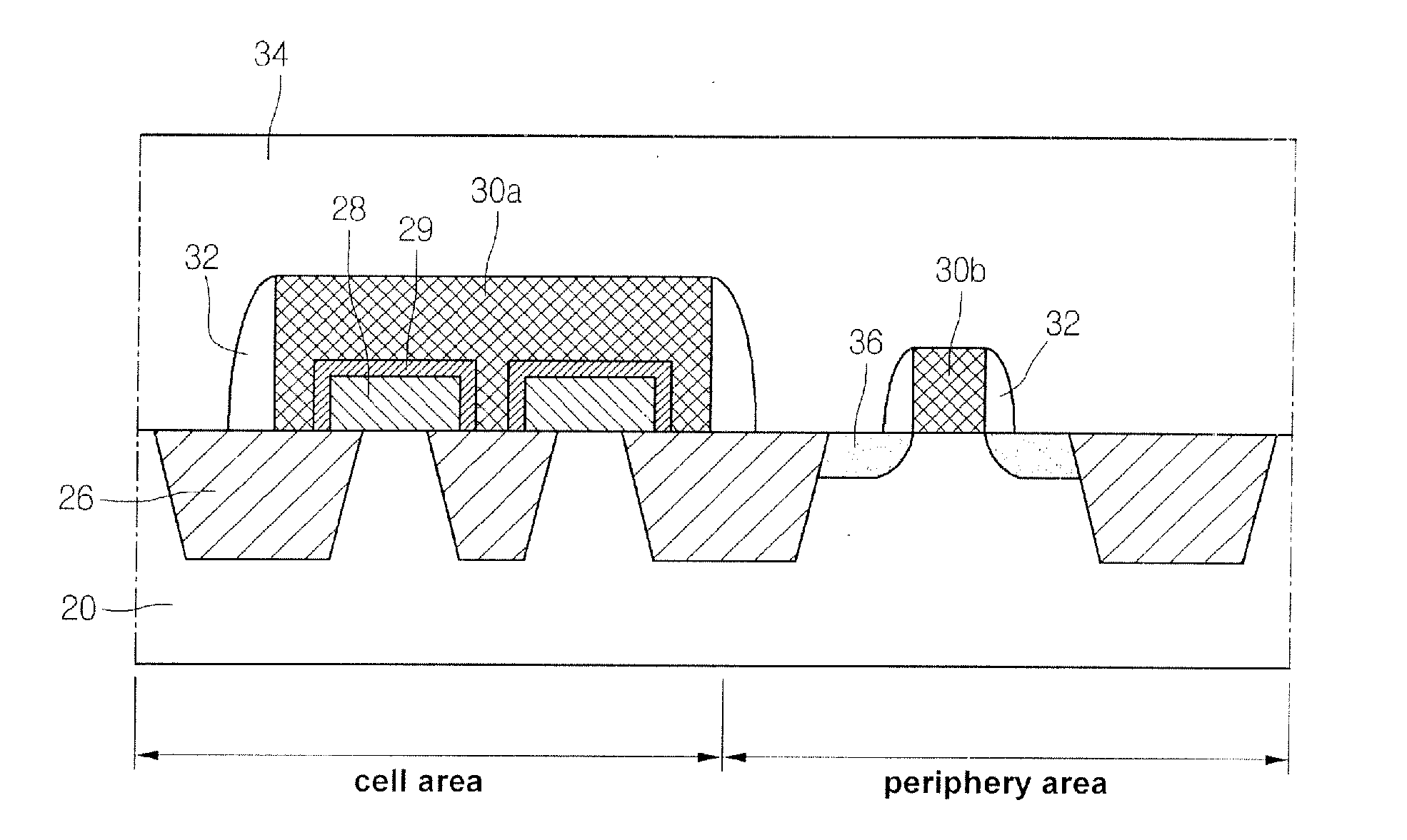
[0028]The semiconductor memory device can have a cell area and a periphery area, where data write and erase operations are performed in the cell area and a transistor is operated in the periphery area corresponding to the data write and erase operations.

[0029]First, after forming a photoresist pattern (not shown) to define an area for an isolation layer on a semiconductor substrate 20, a trench can be formed through an etch process.

[0030]Thereafter, a wet etch process can be performed to remove the photoresist pattern, and then an annealing process is performed with respect to the resultant structure.

[0031]The annealing process can be performed by using a nitrogen (N2) gas under a temperature of about 1100° C. or about 1200° C. for about 5 minutes to about 15 minutes.

[0032]After the annealing pro...

second embodiment

[0058]Hereinafter, a method for manufacturing a semiconductor memory device will be described.

[0059]A semiconductor memory device manufactured through the method according to the second embodiment employs components similar to those of the semiconductor memory device manufactured through the method according to the first embodiment. Therefore, repeated details will be omitted in order to avoid redundancy.

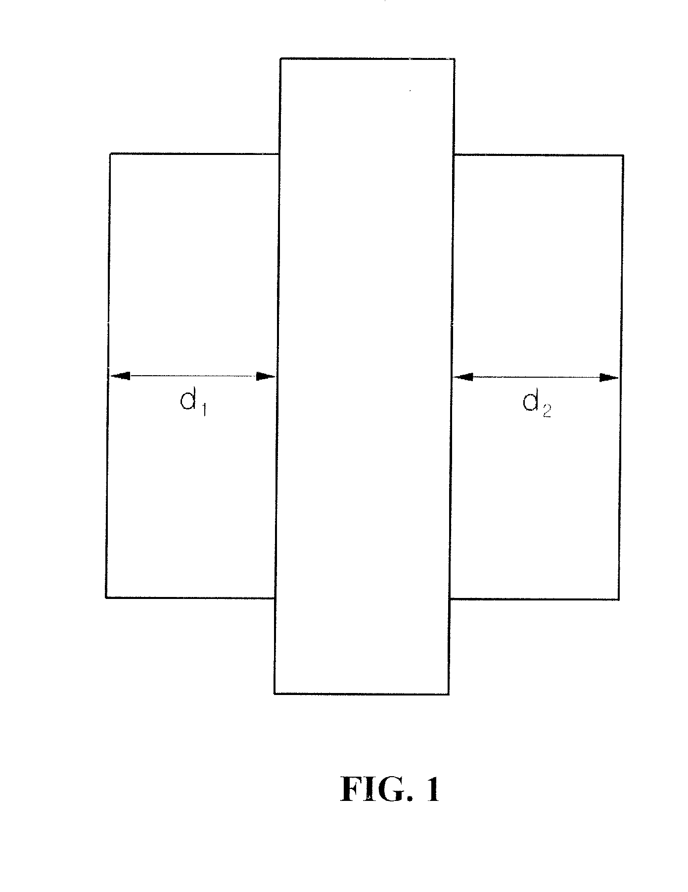
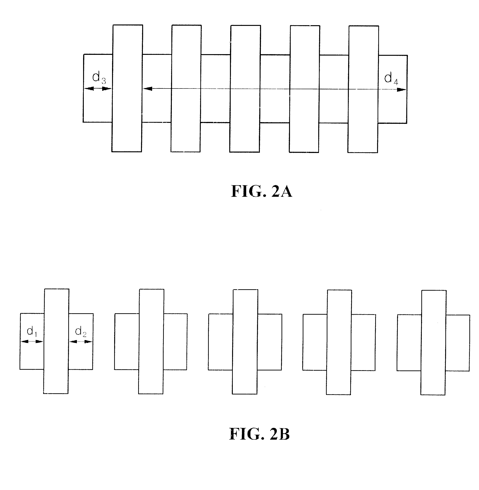
[0060]According to the method for manufacturing the semiconductor memory device of the second embodiment, a line critical dimension (CD) is increased when forming an active layer, thereby minimizing the influence of stress exerted on the active layer.

[0061]FIG. 6 is a view schematically showing the line CD in the semiconductor memory device manufactured through the method according to the second embodiment and the semiconductor memory device manufactured according to the POR.

[0062]Two semiconductor wafers E and F shown in FIG. 6 are manufactured using the same semiconductor process...


PUM

PropertyMeasurementUnit
temperatureaaaaaaaaaa
voltagesaaaaaaaaaa
voltagesaaaaaaaaaa

Abstract

Disclosed are methods for manufacturing a semiconductor memory device. According to an embodiment, a method includes forming a trench to form an isolation layer performing an annealing process to reduce an amount of a leakage current in an active layer, and performing a gap-fill process with respect to the trench. Another method in accordance with an embodiment includes performing a lithography process to form an active layer, in which a line critical dimension (CD) in the active layer is increased by about 3 nm to about 6 nm as compared with a line CD in a Process of Record (POR).

Description

CROSS-REFERENCE TO RELATED APPLICATION[0001]The present application claims the benefit under 35 U.S.C. §119 of Korean Patent Application No. 10-2008-0052951, filed Jun. 5, 2008, which is hereby incorporated by reference in its entirety.BACKGROUND[0002]Stress on an active layer is an important factor for characteristics of a semiconductor device. In particular, the stress applied to the active layer exerts a significant influence upon driving current and leakage current characteristics of the semiconductor device. As the semiconductor device becomes highly integrated, semiconductor layers such as the active layer are scaled down and the stress applied to the active layer is increased.[0003]For example, as the NOR flash device is further integrated, the number of bit cells included in one bit line is increased, and the size of the bit cell (i.e., the pattern size of an active layer, a floating gate, and a control gate, which constitute one flash device) is scaled down. Thus, a bit lin...

Claims


Application Information

Patent Timeline
Patent Type & Authority Applications(United States)
IPC IPC(8): H01L21/762G03F7/20
CPCH01L21/76224H01L21/76H01L21/324
Inventor HONG, JI HO
Owner DONGBU HITEK CO LTD
Why Eureka
Try Eureka