Manufacturing method for electron-emitting device, electron source, and image-forming apparatus

a manufacturing method and technology of an electron-emitting device, applied in the manufacture of electrode systems, electrodes, electrode tubes/lamps, etc., can solve the problems of photo-lithographic processes, extremely high cost, irregular etc., and achieve the goal of reducing the thickness of electroconductive films and minimizing the irregularity of electrical properties such as sheet resistance values

Inactive Publication Date: 2005-09-20
CANON KK
View PDF19 Cites 2 Cited by
  • Summary
  • Abstract
  • Description
  • Claims
  • Application Information

AI Technical Summary

Benefits of technology

[0024]The present invention has been made in view of the aforementioned problems, and the object thereof is to prevent the following: seepage of droplets owing to printed electrodes; or non-uniform spreading of the droplets due to wettage distribution upon the substrate or difference in wettage between the substrate and the electrodes; or precipitation of crystals due to the difference in time from the droplet deposition to the baking process and volatilization or sublimation; thereby developing a manufacturing method for an electron-emitting device of which the thinning of the electroconductive film can be lessened and irregularities in electrical properties such as sheet resistance value can be minimized, and to further provide for a manufacturing method for electron sources, display panels, and image-forming apparatuses, using the same method.

Problems solved by technology

Also, while in recent years image forming apparatuses such as display apparatuses which are flat-type display apparatuses employing liquid crystal have become commonplace in the stead of CRT apparatuses, such flat-type display apparatuses employing liquid crystal have problems such as requiring back lightning due to not being emission type, and development of an emission type display apparatus has been awaited.
While the aforementioned surface conduction electron-emitting device can be applied to image-forming apparatuses and other such apparatuses by means of creating and arraying a great number of such surface conduction electron-emitting devices upon a substrate with a wide area, such an arrangement manufactured with known photo-lithographic processes would result in extremely high costs.
However, depositing droplets upon the printed electrodes employing an ink-jet method results in problems such as follows; i.e., in an event where the density of the printed electrode is low, a phenomena may occur where the deposited droplets penetrate into the electrode by capillary action.
This causes the amount and spread of the liquid to be irregular at the gap portion, causing irregularities in the thickness of the electroconductive film after baking, irregularity in film thickness from one device to another, and irregularities in electric properties.
Also, while this is not a problem confined to the ink-jet method, in the event that the surface conditions of the substrate are not uniform or the wettability of printed electrodes and the substrate are not the same, the droplets are repelled, making formation of a uniform film to be difficult.
Consequently, the organic metal compounds contained within the droplets crystallize, which may cause non-conformity in post-baking film thickness of the electroconductive films and irregularity in the resistance of each of the electroconductive films corresponding to each of the devices.
As a result of the known process, wherein the electroconductive thin film of the organic metal compound is heated to a temperature higher than the melting point or the decomposition point thereof in order to obtain an electroconductive film before conducting energization forming, part of the metal contained within the organic metal compound is lost either to volatilization or sublimation, resulting on thinning of the thickness of the obtained thin film of fine particles of metal or metal oxide, and further creating a problematic situation wherein precise control of the film thickness is difficult.
Further yet, in the event where non-volatile organic compounds are employed for formation of the electroconductive film, crystal precipitation and deformation of the droplets occur during the drying process, making for irregularities in the film thickness, again resulting in a problem wherein precise control of the film thickness is difficult.
Moreover, in the manufacturing process of image-forming apparatuses wherein multiple electron-emitting devices are arrayed, difference in the thickness of the formed electron-emitting devices arises owing to the fact that there is difference in the time from when droplets are deposited on each device till the baking process.
Consequently, in surface conduction electron-emitting devices manufactured according to the aforementioned method, there is great irregularity in the thickness of the electroconductive films and electric properties such as sheet resistance value, thereby resulting in occurrence of brightness irregularities and defective products in resultant electron sources, display panels, and image-forming apparatuses, using the electron-emitting devices.

Method used


Image

  • Manufacturing method for electron-emitting device, electron source, and image-forming apparatus
  • Manufacturing method for electron-emitting device, electron source, and image-forming apparatus
  • Manufacturing method for electron-emitting device, electron source, and image-forming apparatus

Examples


embodiment 1

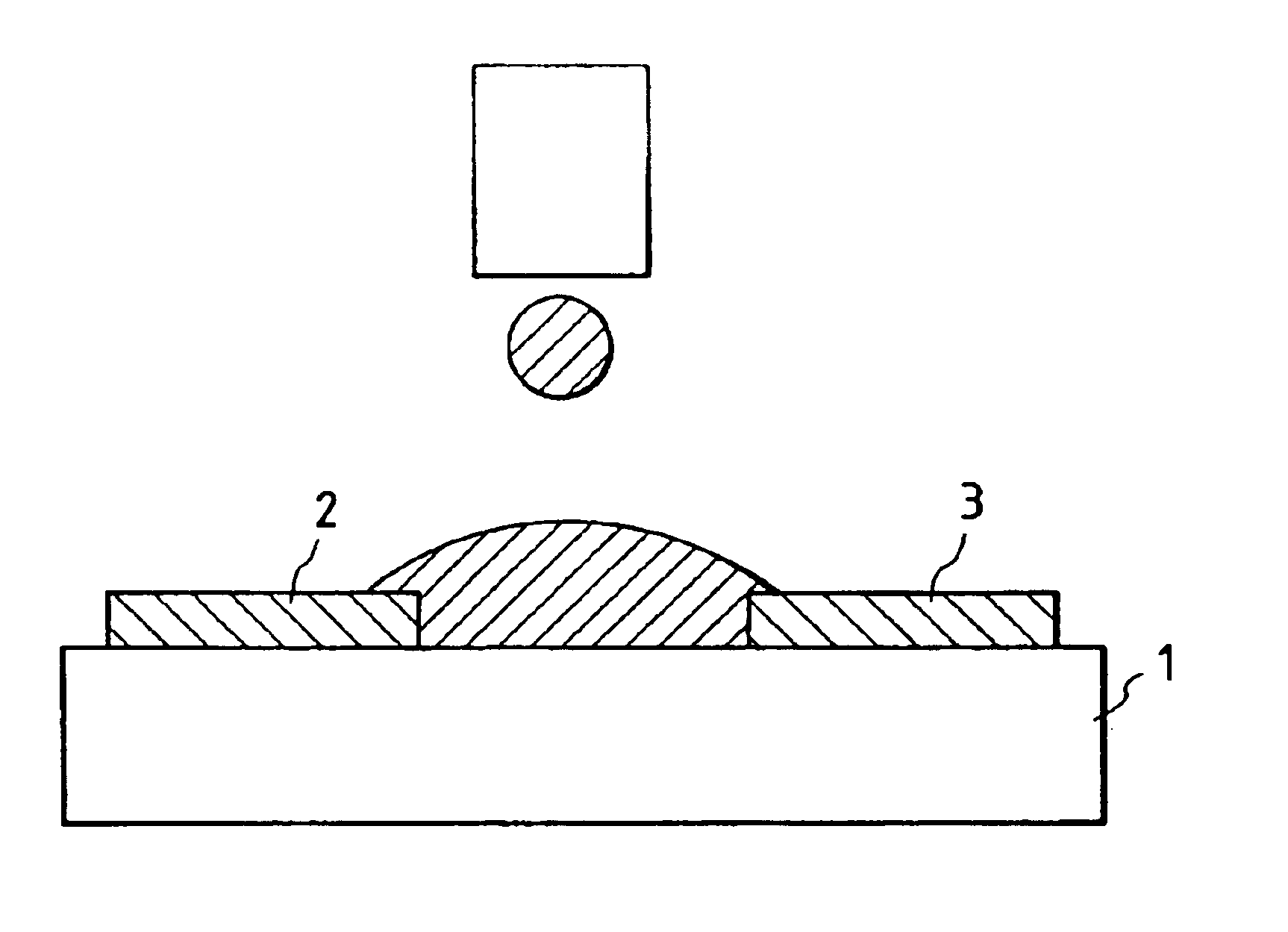
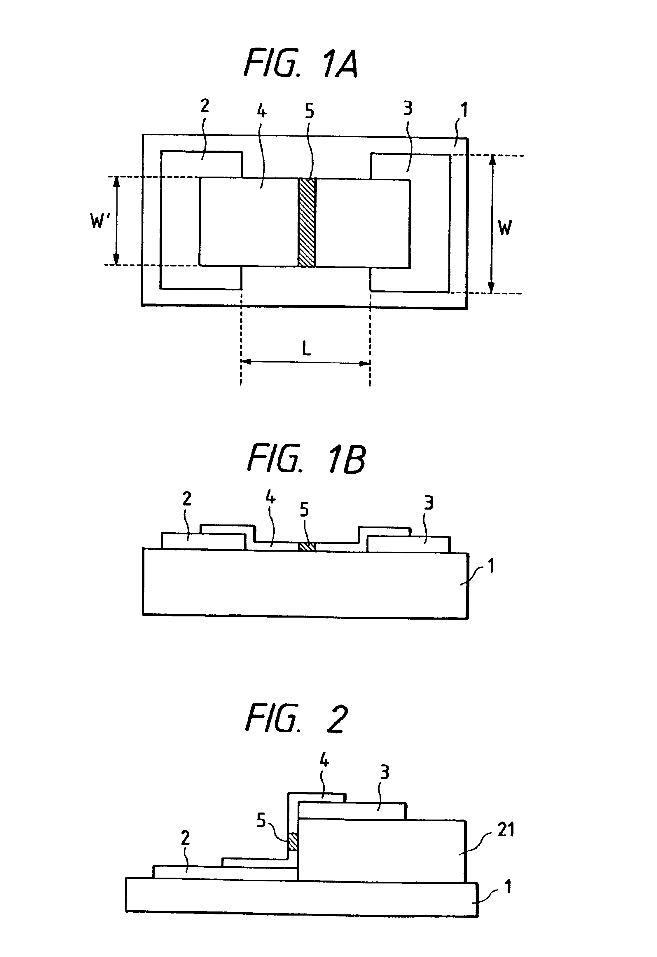
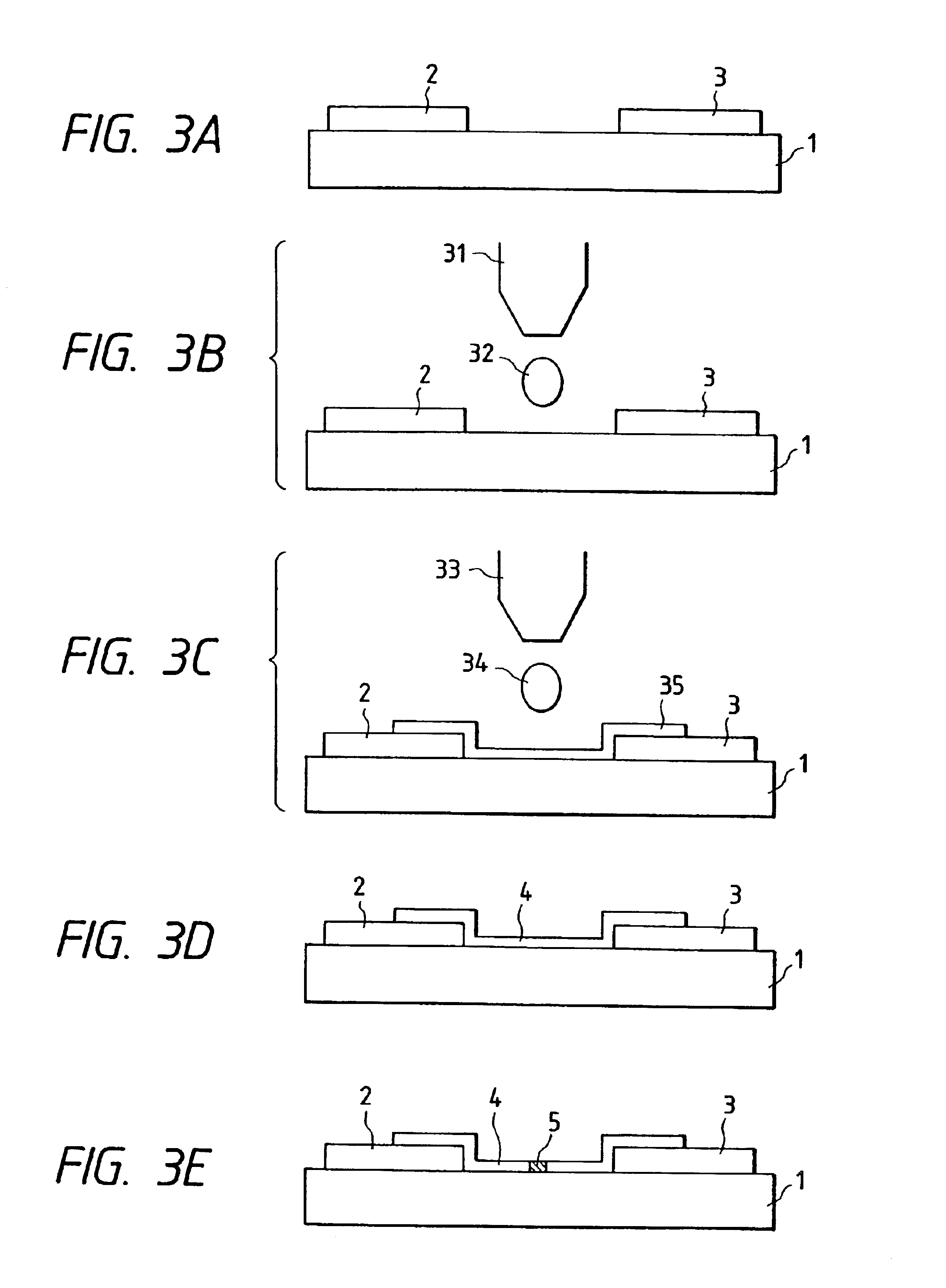
[0180]And electron-emitting device of the type illustrated in FIGS. 1A and 1B was manufactured as an electron-emitting device. FIG. 1A is a plan view illustrating the construction of the present electron-emitting device, and FIG. 1B is a cross-sectional view thereof. In FIGS. 1A and 1B, reference numeral 1 denotes an insulating substrate, reference numerals 2 and 3 denote a pair of device electrodes, reference numeral 4 denotes a film including an electron-emitting region, and reference numeral 5 denotes an electron-emitting region. In the Figures, L represents the spacing between the device electrode 2 and the device electrode 3, W represents the length of the device electrodes, d represents the thickness of the device electrodes, and W′ represents the width of the device.

[0181]The manufacturing method of the electron-emitting device of the present invention will now be described with reference to FIGS. 19A through 19D. A quartz glass plate was used as the insulating substrate 1, a...

embodiment 2

[0194]Polyvinyl alcohol (reffered to PVA) was added to water, and the viscosity of the solution was adjusted to be 5 centipoise in viscosity, which was then deposited onto part of the electrodes by means of a bubble-jet type ink-jet apparatus, then heated at 100° C. for 10 minutes, then cooled to room temperature again. Following this, 100 devices of the present electron-emitting device were fabricated in the same manner as with Embodiment 1. The irregularities in the film thickness of the electroconductive film are shown later in Table 1. Further, when a device voltage was applied between the electrodes 2 and 3 of the present electron-emitting device by means of the measuring / evaluation apparatus described in Embodiment 1, the electron emission under 12V of device voltage was an average of 0.2 μA, and an electron-emission efficiency of 0.05% was obtained. The irregularity of Ie between the devices was 6%.

embodiment 3

[0195]Droplets of the following solutions of aqueous resin solution and organic metal compound solution were deposited as with the Embodiment 2, and electron-emitting devices 3.1 thorough 3.4 were fabricated. Table 1 shows the evaluation results regarding the film thickness and the distribution thereof. The evaluation method was the same as with the Embodiment 1.


PUM


Abstract

A method for manufacturing an electron-emitting device processing an electroconductive film upon which an electron-emission region is formed is characterized in that the formation process of formation of the electron-emission region includes a process of application of metal compound-containing material and film thickness controlling agent to the substrate.

Description

[0001]This application is a division of Application Ser. No. 09 / 935,588, filed Aug. 24, 2001, now U.S. Pat. No. 6,506,440 which is a division of application Ser. No. 08 / 626,757, filed Apr. 2, 1996, now U.S. Pat. No. 6,296,896 B1, issued Oct. 2, 2001.BACKGROUND OF THE INVENTION[0002]1. Field of the Invention[0003]The present invention relates to the manufacturing method of an electron-emitting device, and more particularly, to electron sources, display panels, and image forming apparatuses, employing the aforementioned electron image device.[0004]2. Related Background Art[0005]Conventionally, two types of electron emission devices have been known; i.e., thermionic type and cold cathode type. Types of cold cathode electron-emitting devices include; field emission type devices (hereafter referred to as “FE type device”), metal / insulator / metal type devices (hereafter referred to as “MIM device”), surface conduction electron-emitting devices (hereafter referred to as “SCE device”), etc.[...

Claims


Application Information

Patent Timeline
Patent Type & Authority Patents(United States)
IPC IPC(8): H01J9/02
CPCH01J9/027B05D5/12
Inventor TAKAHASHI, YASUOMIURA, NAOKO
Owner CANON KK
Why Eureka
Try Eureka