Wafer processing deposition shielding components

a shielding component and wafer technology, applied in electrolysis components, vacuum evaporation coatings, coatings, etc., can solve the problems of poor coverage in the bottom and sidewalls of high aspect ratio features, poor conformation of thin films, and use of prior art collimators, etc., to achieve the effect of higher aspect ratio

Inactive Publication Date: 2009-12-17
APPLIED MATERIALS INC
View PDF16 Cites 74 Cited by
  • Summary
  • Abstract
  • Description
  • Claims
  • Application Information

AI Technical Summary

Problems solved by technology

However, with PVD it is difficult to form a uniform, thin film that conforms to the shape of a substrate where a step occurs, such as a via or trench formed in the substrate.
In particular, the broad angular distribution of depositing sputtered atoms leads to poor coverage in the bottom and sidewalls of high aspect ratio features, such as vias and trenches.
However, certain problems exist with the use of prior art collimators in conjunction with small magnet magnetrons.
Unfortunately, PVD with a prior art collimator in combination with a small magnet magnetron provides non-uniform deposition across a substrate.
This phenomenon not only leads to non-uniform deposition across the substrate, but it also leads to non-uniform deposition across high aspect ratio feature sidewalls in certain regions of the substrate as well.

Method used


Image

  • Wafer processing deposition shielding components
  • Wafer processing deposition shielding components
  • Wafer processing deposition shielding components

Examples


Embodiment Construction

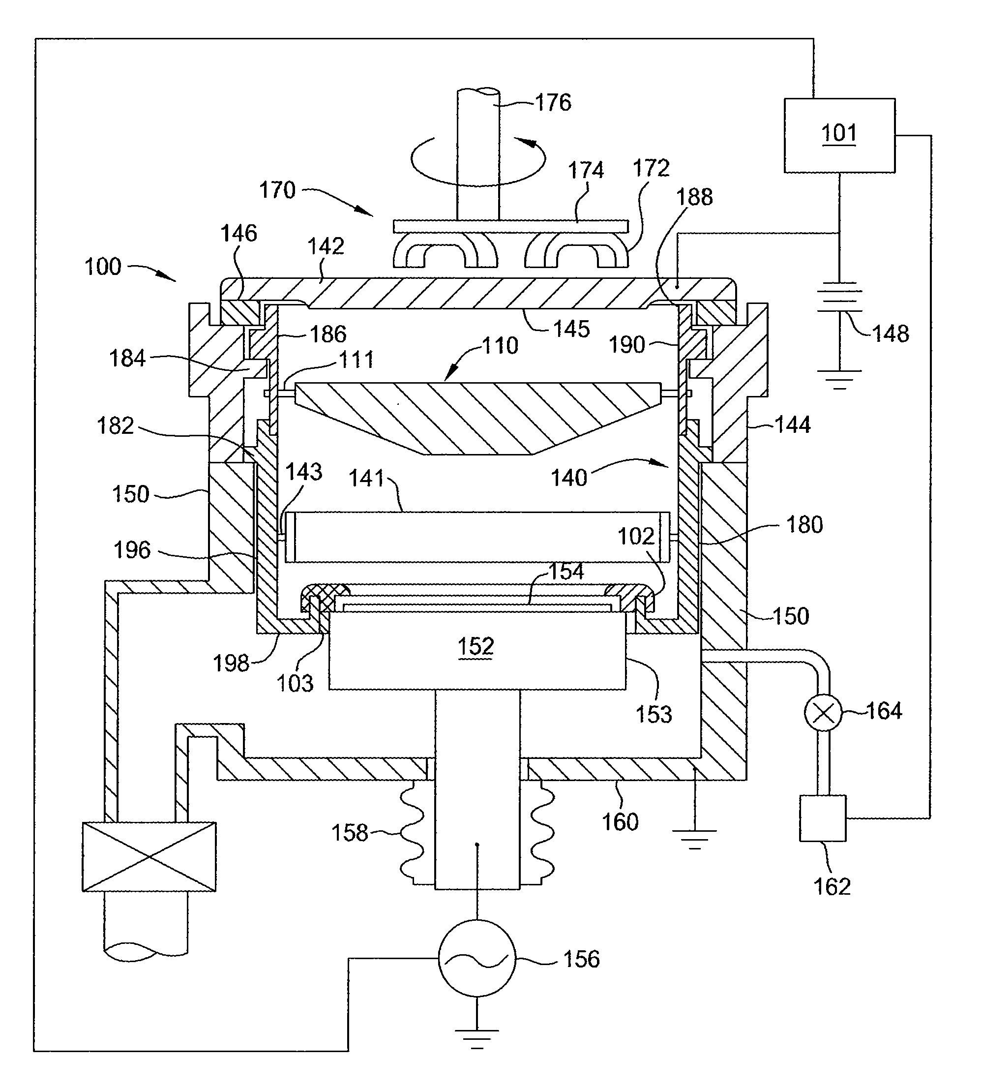
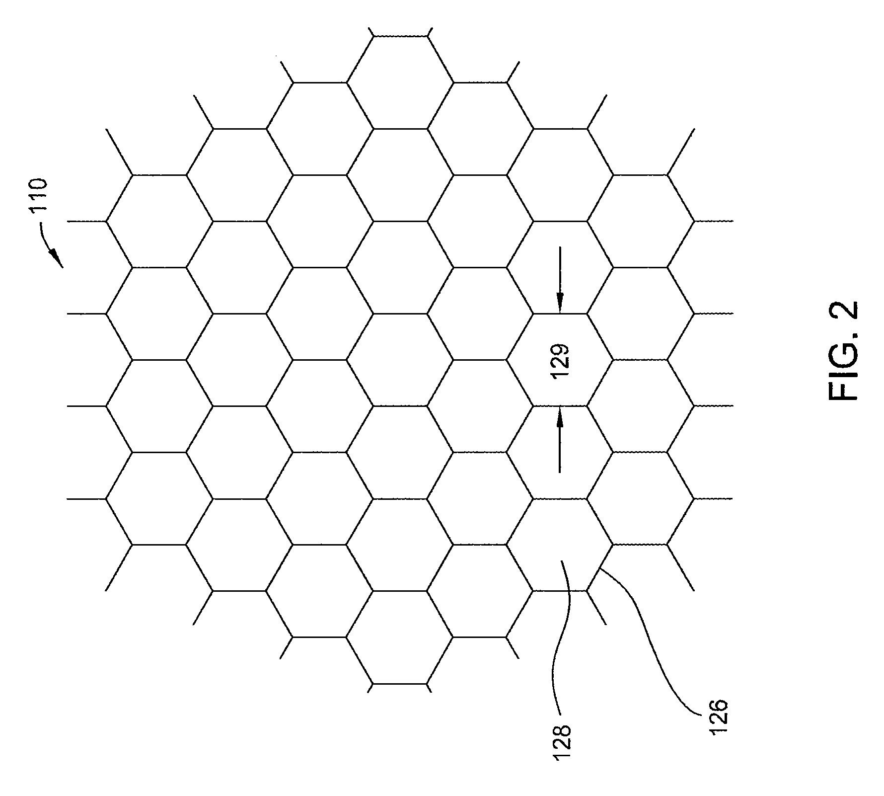
[0030]Embodiments described herein provide apparatus and methods for uniform deposition of sputtered material across high aspect ratio features of a substrate during the fabrication of integrated circuits on substrates.

[0031]FIG. 1 depicts an exemplary embodiment of a processing chamber 100 having one embodiment of a process kit 140 capable of processing a substrate 154. The process kit 140 includes a one-piece lower shield 180, a one-piece upper shield 186, and a collimator 110. In the embodiment shown, the processing chamber 100 comprises a sputtering chamber, also called a physical vapor deposition (PVD) chamber, capable of depositing, for example, titanium, aluminum oxide, aluminum, copper, tantalum, tantalum nitride, tungsten, or tungsten nitride on a substrate. Examples of suitable PVD chambers include the ALPS® Plus and SIP ENCORE® PVD processing chambers, both commercially available from Applied Materials, Inc., Santa Clara, of Calif. It is contemplated that processing chamb...


PUM

PropertyMeasurementUnit
aspect ratioaaaaaaaaaa
thicknessaaaaaaaaaa

Abstract

Embodiments described herein generally relate to an apparatus and method for uniform sputter depositing of materials into the bottom and sidewalls of high aspect ratio features on a substrate. In one embodiment, a collimator for mechanical and electrical coupling with a shield member positioned between a sputtering target and a substrate support pedestal is provided. The collimator comprises a central region and a peripheral region, wherein the collimator has a plurality of apertures extending therethrough and where the apertures located in the central region have a higher aspect ratio than the apertures located in the peripheral region.

Description

CROSS-REFERENCE TO RELATED APPLICATIONS[0001]This application claims benefit of U.S. provisional patent application Ser. No. 61 / 073,130 (Attorney Docket No. 12996L), filed Jun. 17, 2008, and U.S. provisional patent application Ser. No. 61 / 172,627 (Attorney Docket No. 14278L), filed Apr. 24, 2009, both of which are herein incorporated by reference in their entirety. This application is related to U.S. patent application Ser. No. 12 / 482,713, filed Jun. 11, 2009 (Attorney Docket No. 12996).BACKGROUND[0002]1. Field[0003]Embodiments of the present invention generally relate to an apparatus and method for uniform sputter depositing of materials into the bottom and sidewalls of high aspect ratio features on a substrate.[0004]2. Description of the Related Art[0005]Sputtering, or physical vapor deposition (PVD), is a widely used technique for depositing thin metal layers on substrates in the fabrication of integrated circuits. PVD is used to deposit layers for use as diffusion barriers, seed...

Claims


Application Information

Patent Timeline
Patent Type & Authority Applications(United States)
IPC IPC(8): C23C14/34
CPCH01J37/3447H01J37/34
Inventor RIKER, MARTIN LEEEWERT, MAURICE E.SUBRAMANI, ANANTHA K.
Owner APPLIED MATERIALS INC
Why Eureka
Try Eureka