Switching device, semiconductor device, programmable logic integrated circuit, and memory device

a technology of programmable logic and semiconductors, applied in semiconductor devices, bulk negative resistance effect devices, electrical appliances, etc., can solve the problems of shortening the service life of interconnections, deteriorating interconnections, metal contamination, etc., to prevent metal ions from being absorbed, prevent metal ions, and high reliability

Active Publication Date: 2009-12-17
NEC CORP
View PDF3 Cites 30 Cited by
  • Summary
  • Abstract
  • Description
  • Claims
  • Application Information

AI Technical Summary

Benefits of technology

[0019]According to the present invention, since the first electrode for supplying the metal ions is embedded in the opening in the insulating layer having a diffusion prevention function, metal is prevented from being diffused and leaking from side surfaces of the electrode. Therefore, the switching device is effectively prevented from being contaminated by metal. As a result, the switching device is more effective to prevent metal ions from being diffused and leaking out than related devices. Consequently, the switching device according to the present invention and a semiconductor device which employs the switching device are high in reliability and can be used stably over a long period of time.

Problems solved by technology

However, since the above process is accompanied by the movement of ions, the ions may leak out of the switch, causing a metal contamination, unless properly controlled when the switch performs its switching operation.
For example, if a switching device based on the ion conduction is provided in the multilayer interconnection structure of a semiconductor device, then when metal ions leak out of the switching device, the metal ions are diffused into interlayer insulating films, tending to deteriorate interconnections and insulation between vias and shorten the service life of the interconnections.

Method used


Image

  • Switching device, semiconductor device, programmable logic integrated circuit, and memory device
  • Switching device, semiconductor device, programmable logic integrated circuit, and memory device
  • Switching device, semiconductor device, programmable logic integrated circuit, and memory device

Examples


first exemplary embodiment

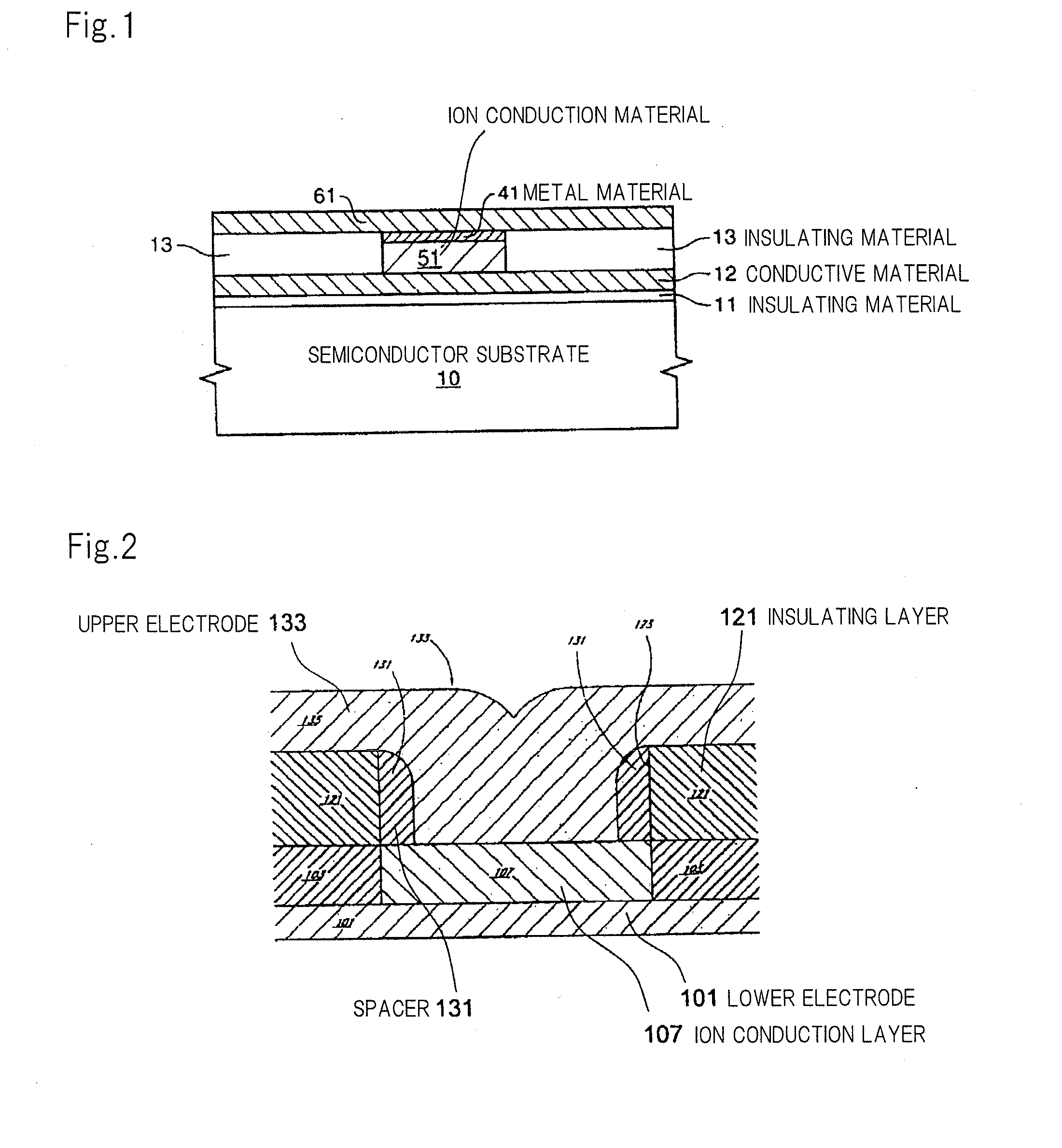
[0056]The configuration of a switching device according to the present exemplary embodiment will be described below. The switching device according to the present exemplary embodiment comprises a two-terminal switch. FIG. 3 is a cross-sectional view showing a configurational example of the switching device according to the present exemplary embodiment. As shown in FIG. 3, the switching device comprises first insulating layer 1003 having an opening, first electrode 104 embedded in the opening, ion conduction layer 105 disposed in contact with the upper surface of first electrode 104, and second electrode 106 disposed in contact with the upper surface of ion conduction layer 105. In FIG. 3, first electrode 104, ion conduction layer 105, and second electrode 106 are stacked on a base body. The ion conduction layer is also referred to as an ion conductor or a solid-state electrolytic layer. The term “ion conduction layer” or “ion conductor” will be used below.

[0057]First electrode 104 i...

example 1

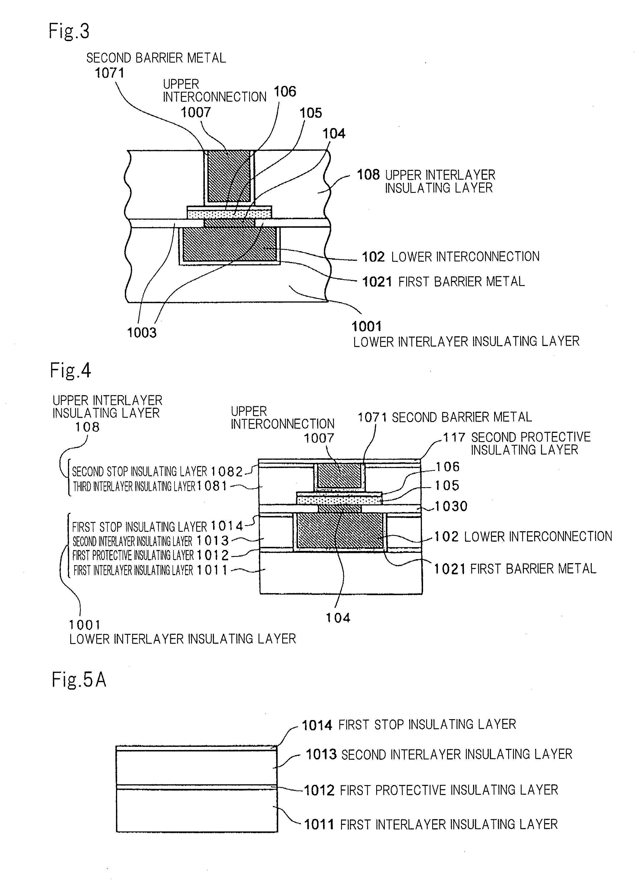
[0092]The present example represents a configurational example of the switching device according to the first exemplary embodiment. FIG. 4 is a cross-sectional view showing the configuration of a switching device according to the first example.

[0093]As shown in FIG. 4, the switching device is basically the same structure as the structure shown in FIG. 3. The switching device includes, on a base body for providing a multilayer interconnection structure, first electrode 104 embedded in an opening in diffusion prevention layer 1030 which corresponds to first insulating layer 1003 shown in FIG. 3, ion conduction layer 105 disposed in contact with the upper surface of first electrode 104, and second electrode 106 covering the upper surface of ion conduction layer 105. The opening in diffusion prevention layer 1030 comprises a through hole as with the structure shown in FIG. 3.

[0094]The base body on which the switching device is disposed comprises a silicon substrate (not shown), semicond...

example 2

[0104]The present example represents a first modification of the switching device according to the first exemplary embodiment. FIG. 6 is a cross-sectional view showing the configuration of a switching device according to the present example. According to the present example, second electrode 106 covers all the side and upper surfaces of ion conduction layer 105. This structure is effective to prevent copper ions dissolved into the ion conduction layer from being diffused laterally and leaking out of the ion conduction layer.

[0105]The structure according to the present example can be produced by modifying [Step D] of Example 1 as follows:

[0106][Step D-1: Formation of the ion conduction layer and the second electrode] A tantalum oxide layer for forming ion conduction layer 105 is deposited to a thickness of 15 nm on first electrode 104 by the sputtering or CVD process. Using the photolithographic technology and the etching technology, ion conduction layer 105 is processed into a shape...


PUM


Abstract

A typical switching device according to the present invention comprises first insulating layer 1003 having an opening and made of a material for preventing metal ions from being diffused, first electrode 104 disposed in the opening and including a material capable of supplying the metal ions, ion conduction layer 105 disposed in contact with an upper surface of the first electrode 104 and capable of conducting the metal ions, and second electrode 106 disposed in contact with an upper surface of the ion conduction layer 105 and including a region made of a material incapable of the metal ions. A voltage is applied between the first electrode 104 and the second electrode 106 for controlling a conduction state between the first electrode 104 and the second electrode 106.

Description

TECHNICAL FIELD [0001]The present invention relates to a switching device employing an ion conductor, a method of manufacturing same, a semiconductor device, a programmable logic integrated circuit, and a memory device which employ such a switching device.BACKGROUND ART [0002]At present, electronic devices have many integrated circuits in use. The many integrated circuits used in the electronic devices are so-called application-specific integrated circuits (ASIC) that are dedicated circuits designed for use in those electronic devices. After an application-specific integrated circuit has been manufactured, its circuit configurations cannot be changed because logic cells (logic circuits serving as units, such as AND circuits and OR circuits) are laid out and interconnected in the integrated circuit fabrication process.[0003]Recent years have seen intensive electronic device development races and electronic device miniaturization. Under the circumstances, attention has been directed t...

Claims


Application Information

Patent Timeline
Patent Type & Authority Applications(United States)
IPC IPC(8): H01L45/00
CPCH01L27/24H01L45/085H01L45/1206H01L27/2472H01L45/1266H01L45/146H01L45/1233H10B63/00H10B63/82H10N70/253H10N70/245H10N70/8416H10N70/826H10N70/8833
Inventor SAKAMOTO, TOSHITSUGU
Owner NEC CORP
Why Eureka
Try Eureka