Eureka AIR delivers breakthrough ideas for toughest innovation challenges, trusted by R&D personnel around the world.

Double exposure patterning with carbonaceous hardmask

Inactive Publication Date: 2009-12-17
APPLIED MATERIALS INC
View PDF21 Cites 16 Cited by
  • Summary
  • Abstract
  • Description
  • Claims
  • Application Information

AI Technical Summary

Benefits of technology

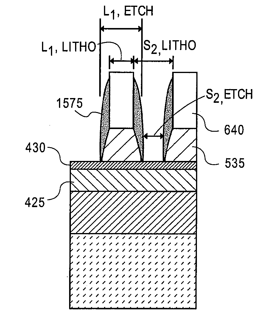
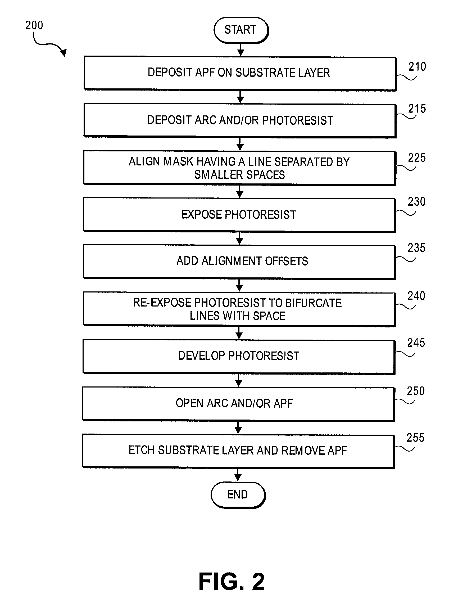
[0010]Multiple exposures of a layer of photoresist are described herein. In one embodiment described, a single reticle may be exposed more than once with an overlay offset implemented between successive exposures to reduce the half pitch of the reticle. In particular embodiments, these methods may be employed to reduce the half pitch of the features printed with 65 nm generation lithography equipment to achieve 45 nm CD and pitch performance.

Problems solved by technology

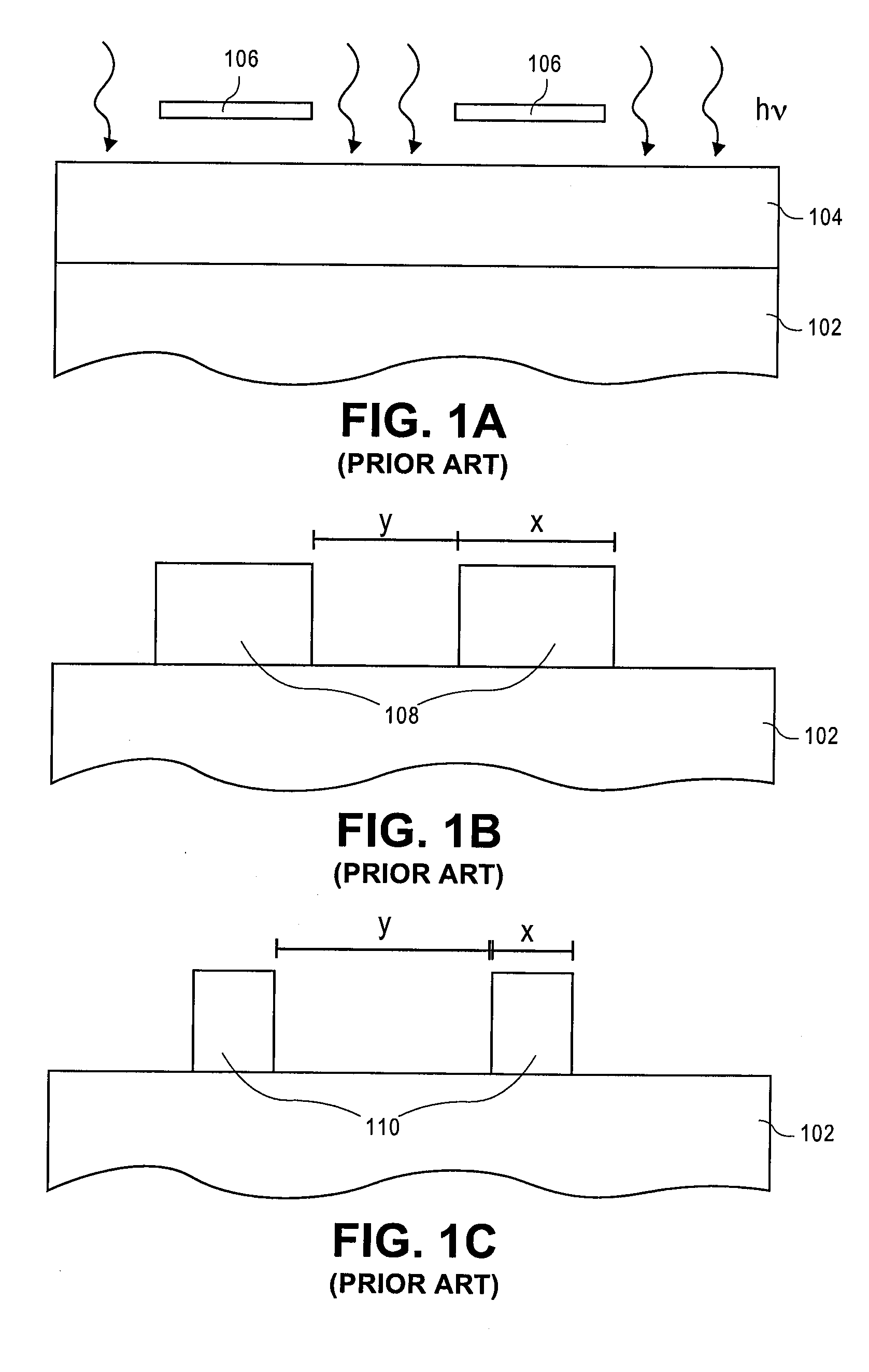
However, such a reduction in feature CD comes at the expense of an increased spacing between features, as depicted by spacing ‘y’ in FIG. 1C.
Progress on these fronts, however, has been slow, hindered by the substantial development and re-tooling required.
DPL however is potentially cost prohibitive, particularly as a result of production cycle time, which increases because multiple photomasks, multiple resist coats and multiple etches are required to form pattern in a single layer.
DPL also incurs an overlay penalty because of the plurality of masking operations.
LER becomes a significant issue when a lithography tool is pushed to image features with minimum CD.

Method used


Image

  • Double exposure patterning with carbonaceous hardmask
  • Double exposure patterning with carbonaceous hardmask
  • Double exposure patterning with carbonaceous hardmask

Examples


Embodiment Construction

[0021]Double exposure methods are described herein with reference to figures. However, particular embodiments may be practiced without one or more of these specific details, or in combination with other known methods, materials, and apparatuses. In the following description, numerous specific details are set forth, such as specific materials, dimensions and processes parameters etc. to provide a thorough understanding of the present invention. In other instances, well-known semiconductor processes and manufacturing techniques have not been described in particular detail to avoid unnecessarily obscuring the present invention. Reference throughout this specification to “an embodiment” means that a particular feature, structure, material, or characteristic described in connection with the embodiment is included in at least one embodiment of the invention. Thus, the appearances of the phrase “in an embodiment” in various places throughout this specification are not necessarily referring...


PUM


Abstract

Methods to pattern features in a substrate layer by exposing a photoresist layer more than once. In one embodiment, a single reticle may be exposed more than once with an overlay offset implemented between successive exposures to reduce the half pitch of the reticle. In particular embodiments, these methods may be employed to reduce the half pitch of the features printed with 65 nm generation lithography equipment to achieve 45 nm lithography generation CD and pitch performance.

Description

BACKGROUND[0001]1. FIELD[0002]Embodiments of the present invention relate to the electronics manufacturing industry and more particularly to a patterning process enabling a reduced half pitch.[0003]2. Discussion of Related Art[0004]Lithography is used in the manufacture of integrated circuits (ICs). FIGS. 1A-1C illustrate cross-sectional views of a conventional semiconductor lithographic process. Referring to FIG. 1A, a photoresist layer 104 is provided above a semiconductor stack 102. A mask or reticle 106 is positioned above photoresist layer 104. A lithographic process includes exposure of photoresist layer 104 to radiation (hν) having a particular wavelength (λ), as indicated by the arrows in FIG. 1A. Referring to FIG. 1B, photoresist layer 104 is subsequently developed to remove the portions photoresist layer 104 that were exposed to light and thereby provide patterned photoresist layer 108 above semiconductor stack 102. The width of each feature of patterned photoresist layer ...

Claims


Application Information

Patent Timeline
IPC IPC(8): G03F7/20
CPCG03F7/091G03F7/2022G03F7/11G03F7/70433G03F7/70466G03F9/70H01L21/0337
Inventor CHEN, HUI W.CHANG, CHORNG-PINGCHEN, YONGMEIDAI, HUIXIONGYU, JIAHUAYANG, SUSIE X.XU, XUMOUBENCHER, CHRISTOPHER D.HUNG, RAYMOND HOIMANDUANE, MICHAEL P.NGAI, CHRISTOPHER SIU WINGSHU, JENMACWILLIAMS, KENNETH
Owner APPLIED MATERIALS INC
Why Eureka
Eureka Blog
Learn More