Thin film transistor and manufacturing method thereof, and display device and manufacturing method thereof

Inactive Publication Date: 2009-12-17
SEMICON ENERGY LAB CO LTD
View PDF15 Cites 21 Cited by
  • Summary
  • Abstract
  • Description
  • Claims
  • Application Information

AI Technical Summary

Benefits of technology

[0043]A pattern of a gate electrode can be formed without using an additional photomask, and the number of steps for manufacturing a thin film transistor can be significantly reduced. The thin film transistor can be applied to a display device. Accordingly, the number of steps for manufacturing a display device can be significantly reduced as well.
[0044]More specifically, the number of photomasks can be reduced. It is also possible to manufacture a thin film transistor using one photomask (multi-tone mask). Accordingly, the number of steps for manufacturing a thin film transistor or a display device can be significantly reduced. Further, a thin film transistor can be manufactured using one photomask, whereby misalignment can be prevented in aligning a photomask.
[0045]In addition, a complicated step using backside light exposure, resist reflow, a lift-off method, or the like is not needed unlike the conventional technique which is aimed at reducing the number of photomasks. Therefore, the number of steps for man

Problems solved by technology

However, even in the case where a bottom gate thin film transistor is manufactured using the above-described mult

Method used


Image

  • Thin film transistor and manufacturing method thereof, and display device and manufacturing method thereof
  • Thin film transistor and manufacturing method thereof, and display device and manufacturing method thereof
  • Thin film transistor and manufacturing method thereof, and display device and manufacturing method thereof

Examples


Example

Embodiment 1

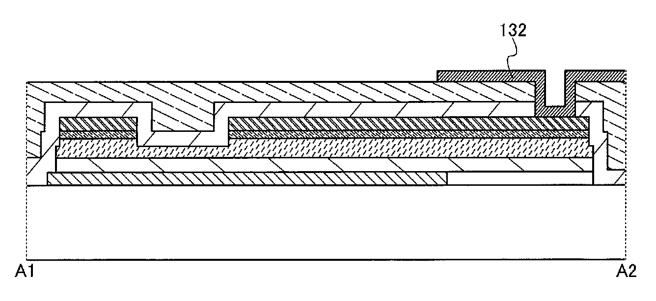
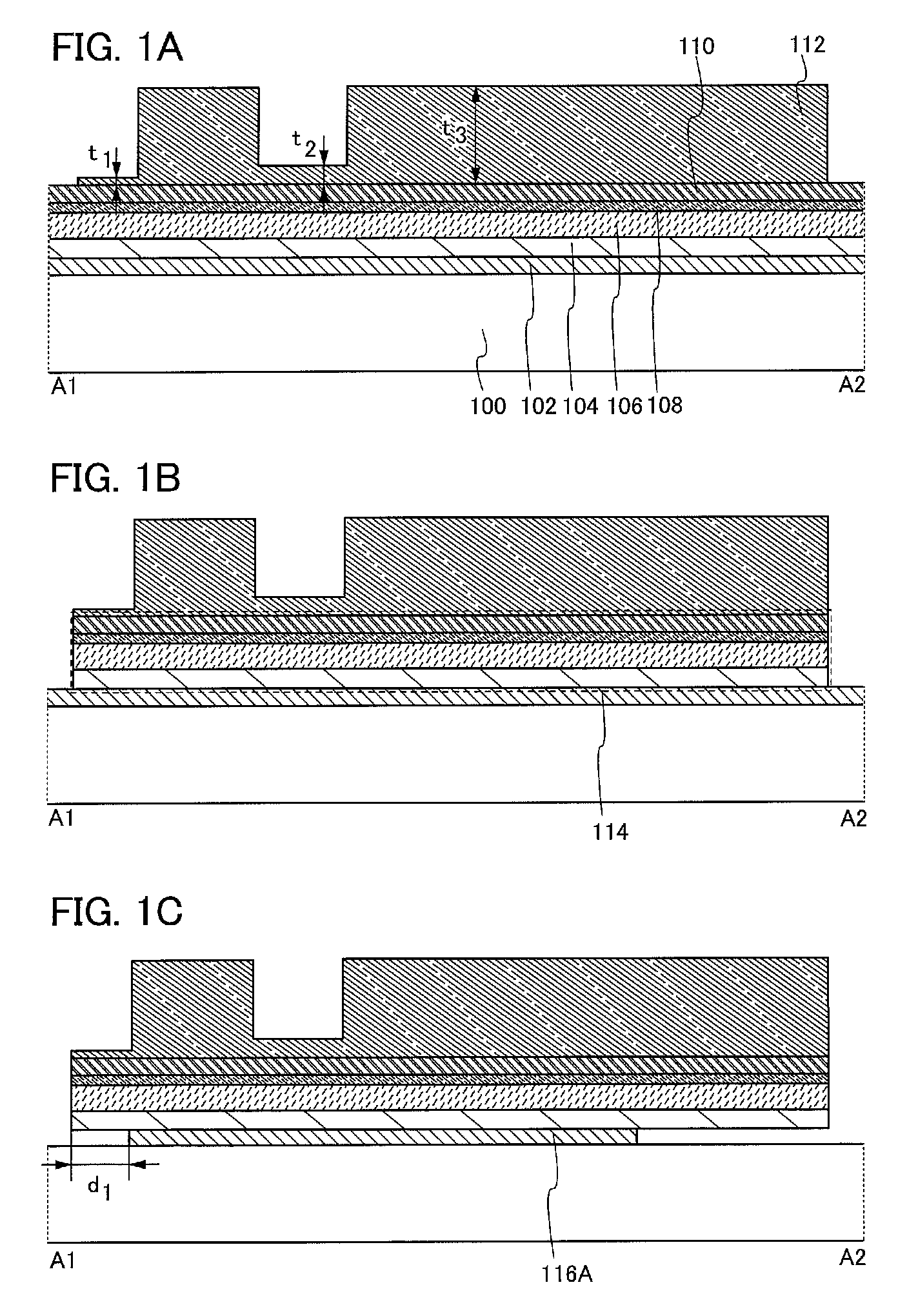
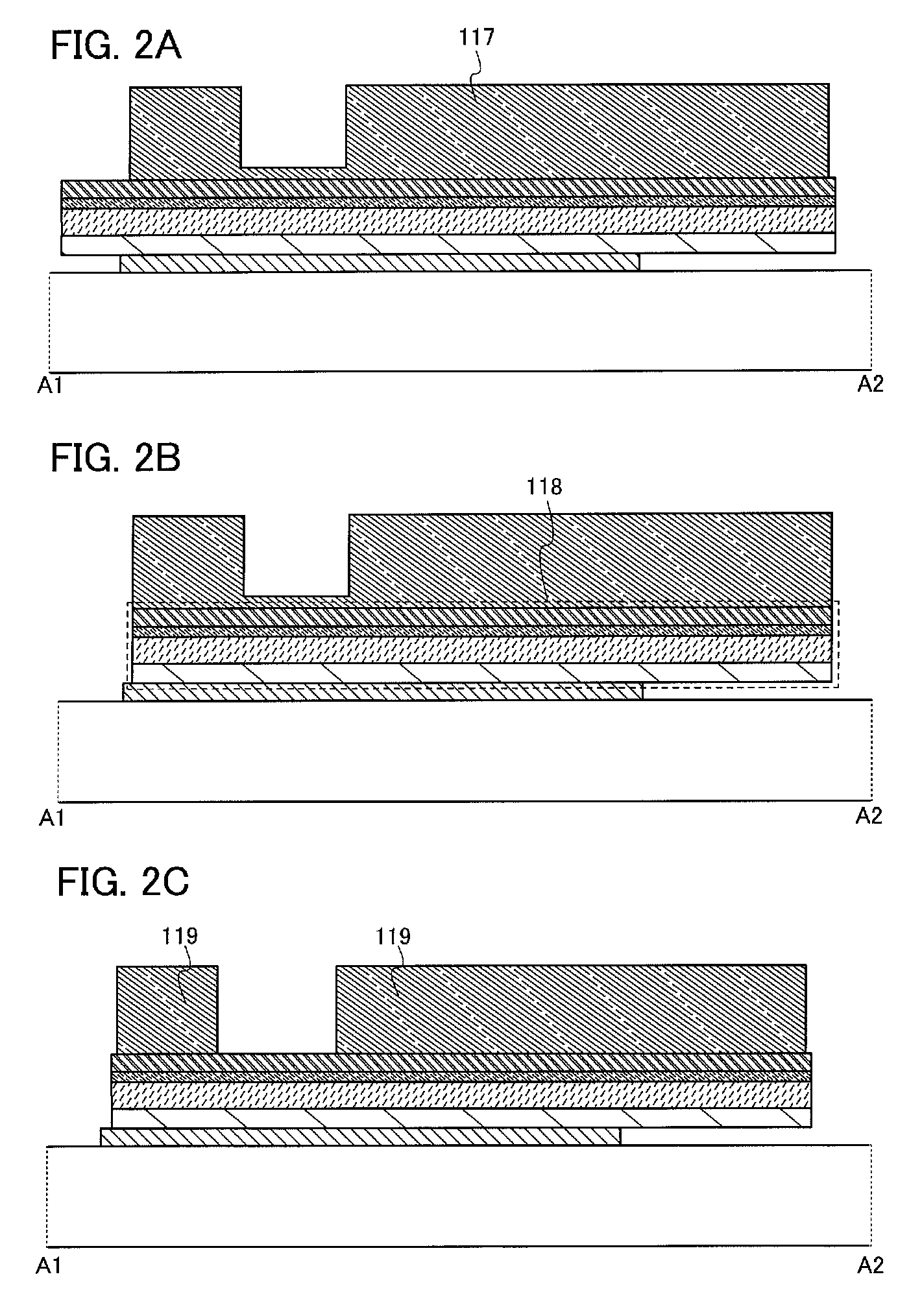
[0103]In this embodiment, an example of a manufacturing method of a thin film transistor and a manufacturing method of a display device in which the thin film transistors are arranged in matrix will be described with reference to FIGS. 1A to 1C, FIGS. 2A to 2C, FIGS. 3A to 3C, FIGS. 4A to 4C, FIGS. 5A to 5C, FIGS. 6A to 6C, FIGS. 7A to 7C, FIGS. 8A to 8C, FIGS. 9A to 9C, FIGS. 10A to 10C, FIGS. 11A to 11C, FIGS. 12A to 12C, FIGS. 13A to 13C, FIGS. 14A to 14C, FIGS. 15A to 15C, FIGS. 16A to 16C, FIGS. 17A to 17C, FIGS. 18A to 18C, FIGS. 19A to 19C, FIGS. 20A to 20C, FIG. 21, FIG. 22, FIG. 23, FIG. 24, FIG. 25, FIG. 26, FIG. 27, FIG. 28, FIG. 29, FIGS. 30A and 30B, FIG. 31, FIG. 32, and FIGS. 33A to 33C.

[0104]Note that FIG. 21, FIG. 22, FIG. 23, FIG. 24, FIG. 25, FIG. 26, FIG. 27, FIG. 28, and FIG. 29 illustrate top views of thin film transistors according to this embodiment, and FIG. 29 is a completion view in the situation that formation of a pixel electrode is finished....

Example

Embodiment 2

[0208]In this embodiment, a manufacturing method of a thin film transistor and a display device, which are different from those of Embodiment 1, will be described.

[0209]Although the case where a resist mask which includes three regions with different thicknesses is formed using a four-tone mask is described in Embodiment 1, a method for forming a resist mask which includes three regions with different thicknesses without using a four-tone mask is described in this embodiment.

[0210]In FIG. 52, the first resist mask 112 (see FIG. 21) in which different hatching patterns are used depending on the thickness is illustrated. The first resist mask 112 includes a first region 171 with the smallest thickness, a third region 173 with the largest thickness, and a second region 172 whose thickness is larger than that of the first region 171 and smaller than that of the third region 173. Note that, here, a molybdenum film, a silicon nitride film, a semiconductor film, an impurity sem...

Example

Embodiment 3

[0222]A thin film transistor which is an embodiment of the present invention can also be applied to an EL display device. In this embodiment, an example of a manufacturing method of a thin film transistor and a manufacturing method of an EL display device in which the thin film transistors are arranged in matrix will be described with reference to FIG. 34, FIGS. 35A to 35C, FIGS. 36A to 36C, FIGS. 37A to 37C, FIGS. 38A to 38C, FIG. 39, FIG. 40, FIG. 41, FIG. 42, FIG. 43, FIG. 44, FIG. 45, FIG. 46, and FIG. 47.

[0223]Various pixel circuits for EL display devices (active EL display devices) which use thin film transistors as switching elements are considered. FIG. 34 illustrates an example of a simple pixel circuit, and a manufacturing method of a pixel structure using this pixel circuit will be described in this embodiment. However, the pixel circuit of the EL display device is not limited to the one having the configuration illustrated in FIG. 34.

[0224]In the pixel struct...


PUM


Abstract

To provide a manufacturing method of a thin film transistor and a display device with fewer masks than a conventional method. A thin film transistor is manufactured by including the steps of: forming a first conductive film, an insulating film, a semiconductor film, an impurity semiconductor film, and a second conductive film to be stacked; forming a resist mask including three regions with different thicknesses; performing first etching to form a thin-film stack body; performing second etching in which side-etching is performed on the thin-film stack body to form a gate electrode layer; and recessing the resist mask to form a semiconductor layer and a source and drain electrode layer. A resist mask including three regions with different thicknesses can be formed using a four-tone photomask, for example.

Description

BACKGROUND OF THE INVENTION[0001]1. Field of the Invention[0002]The present invention relates to a thin film transistor and a manufacturing method thereof, and a display device including the thin film transistor and a manufacturing method thereof.[0003]2. Description of the Related Art[0004]In recent years, thin film transistors that are formed using a semiconductor thin film having a thickness of several nanometers to several hundreds of nanometers over a substrate having an insulating surface such as a glass substrate have been attracting attentions. Thin film transistors are widely used for electronic devices such as ICs (integrated circuits) and electro-optical devices. In particular, thin film transistors are urgently developed as switching elements of image display devices typified by liquid crystal display devices, EL (electro luminescence) display devices, and the like. In an active matrix liquid crystal display device, specifically, voltage is applied to a pixel electrode c...

Claims


Application Information

Patent Timeline
IPC IPC(8): H01L33/00H01L21/336G02F1/1368H01L29/417H01L29/423H01L29/49H01L29/786H01L51/50
CPCH01L27/1214H01L27/1288H01L29/66757G02F1/1368
Inventor MIYAIRI, HIDEKAZUKOMATSU, RYU
Owner SEMICON ENERGY LAB CO LTD
Why Eureka
Try Eureka