Forming ESD Diodes and BJTs Using FinFET Compatible Processes

a technology of esd diodes and bjts, which is applied in the direction of electrical apparatus, semiconductor devices, semiconductor/solid-state device details, etc., can solve the problems of short duration of esd transient, extreme high voltage development in the vicinity of integrated circuits, and destruction of entire integrated circuits, so as to improve esd current

Inactive Publication Date: 2009-12-24
TAIWAN SEMICON MFG CO LTD
View PDF0 Cites 92 Cited by
  • Summary
  • Abstract
  • Description
  • Claims
  • Application Information

AI Technical Summary

Benefits of technology

[0012]The advantageous features of the present invention include improved ESD currents that m

Problems solved by technology

It is well known that extremely high voltages can develop in the vicinity of an integrated circuit due to the build-up of static charges.
ESD is a serious problem for semiconductor devices since it has the potential of destroying the entire integrated circuit.
The duration of the ESD transient is very short, typically in the order of nanoseconds, and the conventional circuit breakers cannot react quickly enough to provide adequate protection.
T

Method used


Image

  • Forming ESD Diodes and BJTs Using FinFET Compatible Processes
  • Forming ESD Diodes and BJTs Using FinFET Compatible Processes
  • Forming ESD Diodes and BJTs Using FinFET Compatible Processes

Examples


Embodiment Construction

[0016]The making and using of the presently preferred embodiments are discussed in detail below. It should be appreciated, however, that the present invention provides many applicable inventive concepts that can be embodied in a wide variety of specific contexts. The specific embodiments discussed are merely illustrative of specific ways to make and use the invention, and do not limit the scope of the invention.

[0017]A novel electrostatic discharging (ESD) device and the method of forming the same are provided. The intermediate stages of manufacturing embodiments of the present invention are illustrated. The variations of the embodiments are then discussed. Throughout the various views and illustrative embodiments of the present invention, like reference numbers are used to designate like elements.

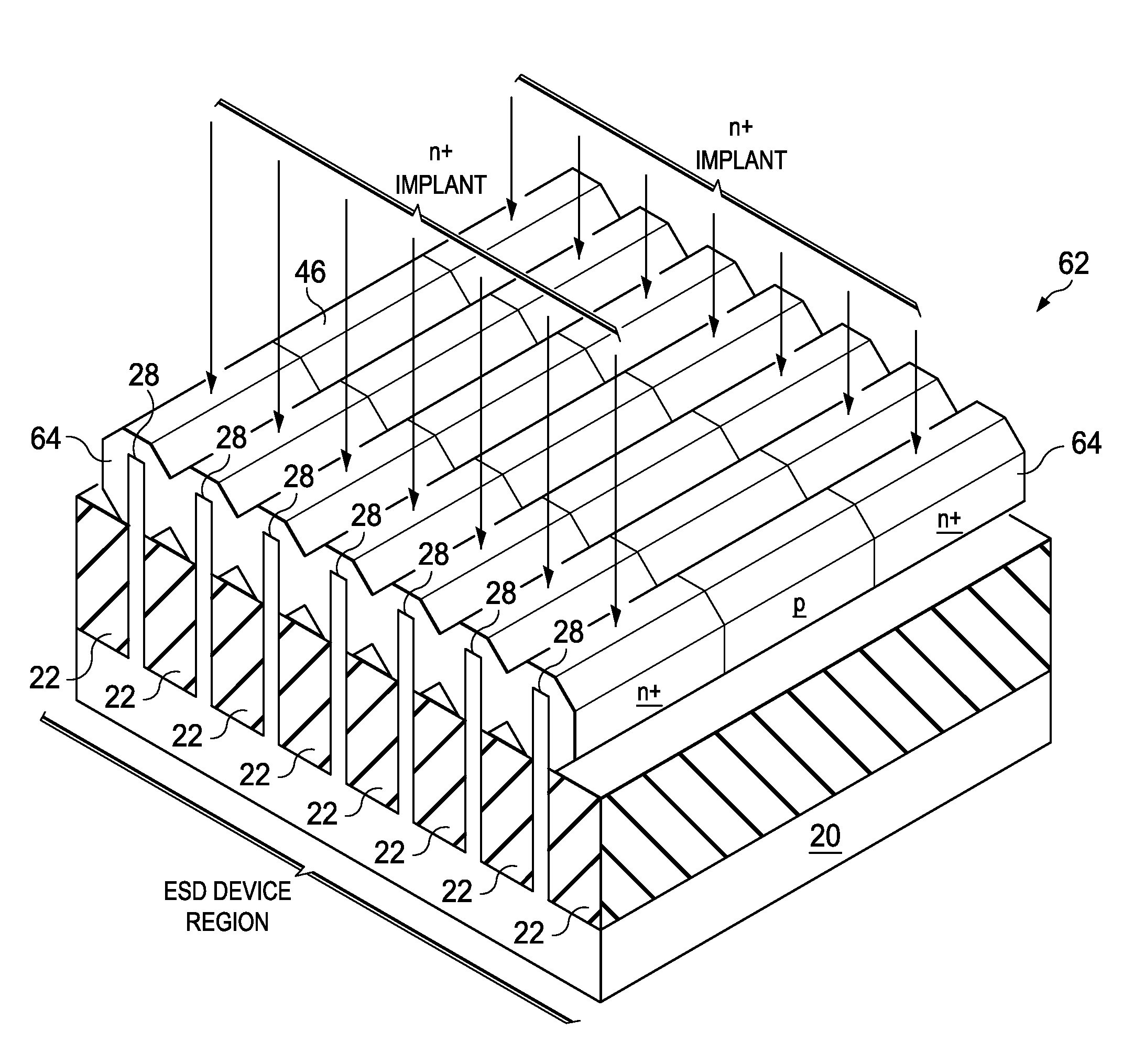
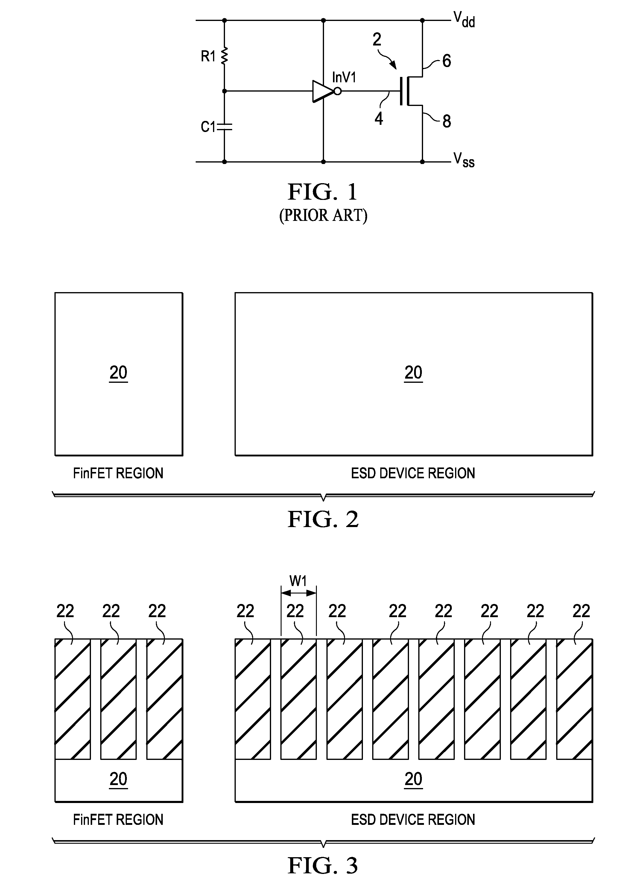
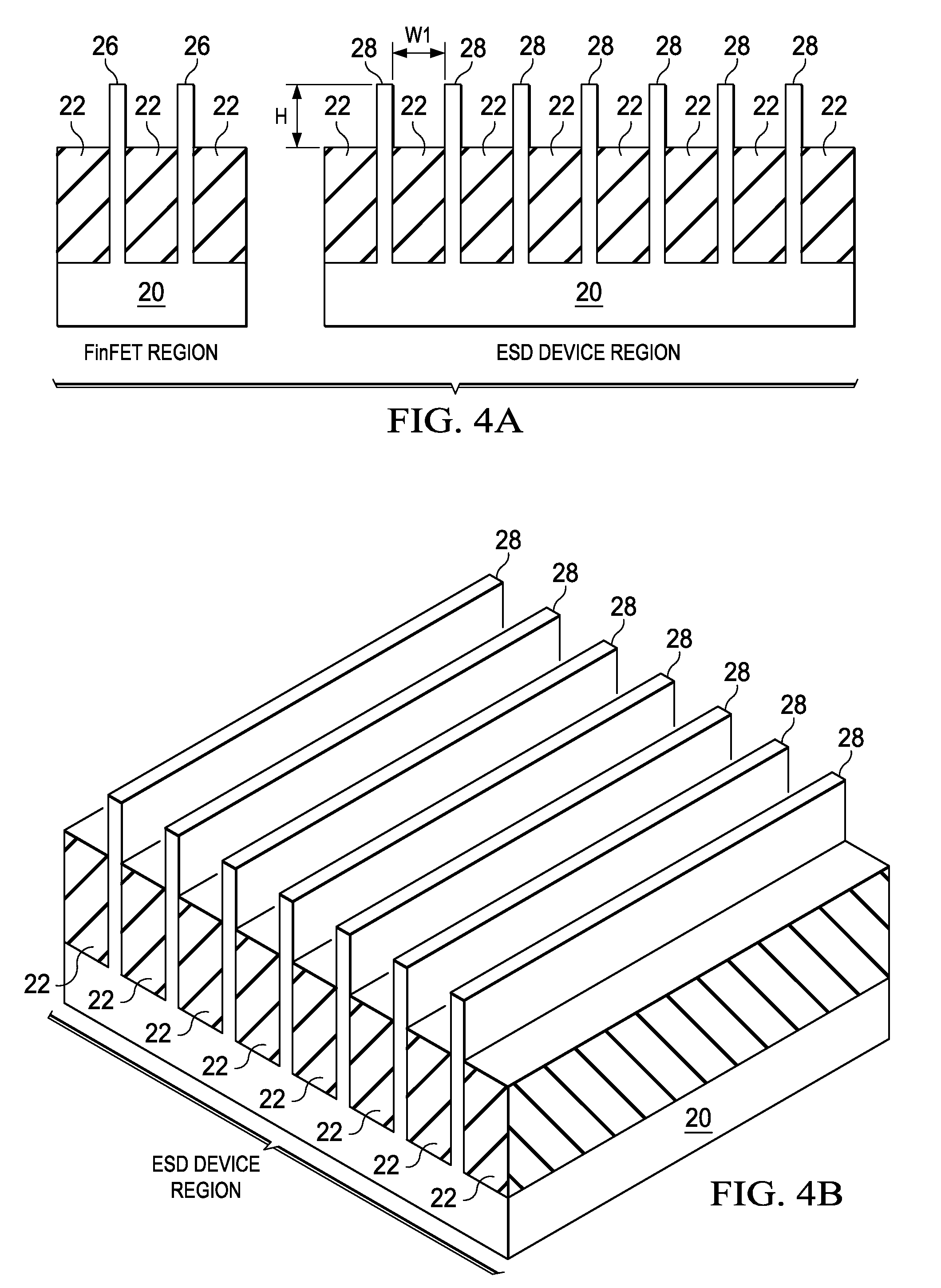
[0018]FIG. 2 illustrates a cross-sectional view of substrate 20, which includes a FinFET region and an ESD device region. The FinFET device region may be a core circuit region, an input / ou...


PUM


Abstract

A method of forming an electrostatic discharging (ESD) device includes forming a first and a second semiconductor fin over a substrate and adjacent to each other; epitaxially growing a semiconductor material on the first and the second semiconductor fins, wherein a first portion of the semiconductor material grown from the first semiconductor fin joins a second portion of the semiconductor material grown from the second semiconductor fin; and implanting a first end and a second end of the semiconductor material and first end portions of the first and the second semiconductor fins to form a first and a second implant region, respectively. A P-N junction is formed between the first end and the second end of the semiconductor material. The P-N junction is a junction of an ESD diode, or a junction in an NPN or a PNP BJT.

Description

TECHNICAL FIELD[0001]This invention relates generally to an electrostatic discharge (ESD) protection circuits, and more particularly to the ESD protection circuits formed using FinFET compatible processes.BACKGROUND[0002]It is well known that extremely high voltages can develop in the vicinity of an integrated circuit due to the build-up of static charges. A high potential may be generated to an input or output buffer of the integrated circuit, which may be caused by a person touching a package pin that is in electrical contact with the input or output buffer. When the electrostatic charges are discharged, a high current is produced at the package nodes of the integrated circuit, and is referred to electrostatic discharge (ESD). ESD is a serious problem for semiconductor devices since it has the potential of destroying the entire integrated circuit.[0003]The duration of the ESD transient is very short, typically in the order of nanoseconds, and the conventional circuit breakers cann...

Claims


Application Information

Patent Timeline
IPC IPC(8): H01L29/00H01L21/336
CPCH01L21/823431H01L29/785H01L29/66795H01L27/0248
Inventor LEE, JAM-WEM
Owner TAIWAN SEMICON MFG CO LTD
Why Eureka
Try Eureka