Photoelectric conversion element and solid-state imaging device

a technology of conversion element and photoelectric layer, which is applied in the direction of solid-state device, semiconductor device, organic semiconductor device, etc., can solve the problems of reducing photoelectric conversion performance, deteriorating photoelectric conversion performance, and stress in the transparent electrode can crack or wrinkle the photoelectric conversion layer, so as to reduce the thickness of the electrode, prevent cracking, and reduce the effect of delamination or deformation

Inactive Publication Date: 2009-12-24
FUJIFILM CORP
View PDF7 Cites 21 Cited by
  • Summary
  • Abstract
  • Description
  • Claims
  • Application Information

AI Technical Summary

Benefits of technology

[0006]JP 9-36406A proposes reducing the electrode thickness to lower the stress generated in the electrode thereby to prevent reduction of performance of a photoelectric conversion element. However, reduction in photoelectric conversion performance is still unavoidable with this method when the photoelectric conversion element has a large area or when the electrode has a large stress even with a reduced thickness.
[0022]The photoelectric conversion element according to the invention has a stress buffer layer at least part of which has a stack structure containing a crystalline sublayer between at least one of the electrodes and the photoelectric conversion layer. The stress buffer layer buffers the stress generated in the electrode. Therefore, cracking, delamination or deformation is prevented from occurring along the interface between the electrode and the photoelectric conversion layer or between the electrode and a blocking layer. The provision of the stress buffer layer eliminates the need to reduce the electrode thickness so that disadvantages that might be otherwise caused by an increased resistance of the electrode, such as reduction in voltage or response speed, are avoided.
[0023]The present invention provides a photoelectric conversion element and a solid state imaging device that are prevented from performance reduction caused by the stress generated in the electrode.

Problems solved by technology

There is concern that the stress generated in the electrode can cause cracking, delamination or deformation at the interface between the electrode and the photoelectric conversion layer or between the electrode and the blocking layer, resulting in deterioration of photoelectric conversion performance.
In particular, in a configuration having a photoelectric conversion layer of an organic material and a transparent electrode, e.g., of ITO formed on the photoelectric conversion layer as a counter electrode, the stress in the transparent electrode can crack or wrinkle the photoelectric conversion layer.
This leads to reduction of photoelectric conversion performance, such as an increase in dark current.
Although the stress of the transparent electrode could be lessened by reducing its thickness, this results in an increase of the resistance of the transparent electrode, which will be followed by remarkable reductions in voltage or response speed especially when the photoelectric conversion element has a large area and invite reduction of the photoelectric conversion performance as a result.
However, reduction in photoelectric conversion performance is still unavoidable with this method when the photoelectric conversion element has a large area or when the electrode has a large stress even with a reduced thickness.

Method used


Image

  • Photoelectric conversion element and solid-state imaging device
  • Photoelectric conversion element and solid-state imaging device
  • Photoelectric conversion element and solid-state imaging device

Examples


first embodiment

[I] First Embodiment

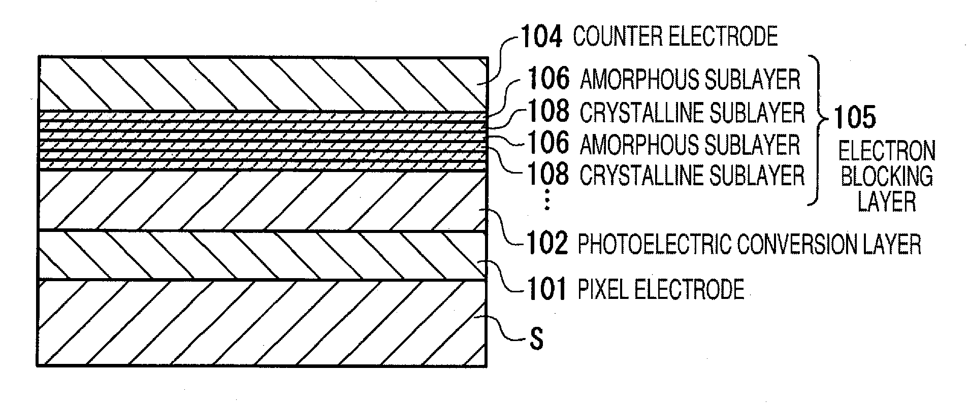
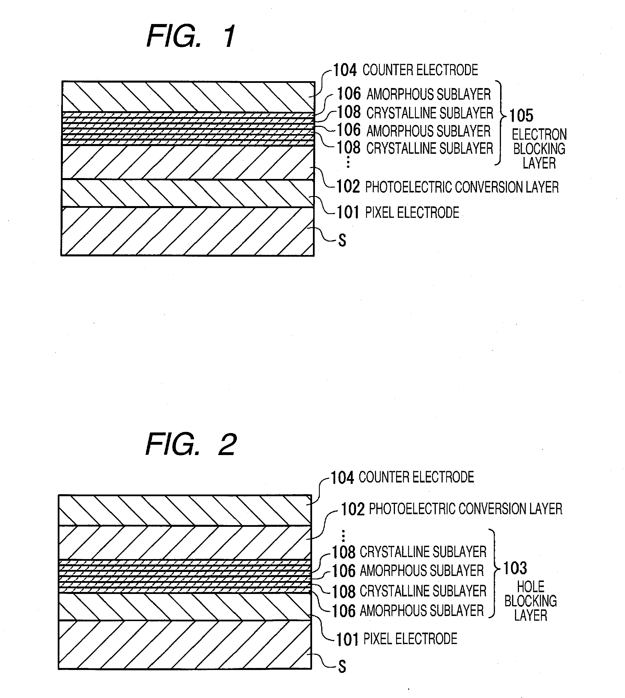
[0031]FIG. 1 is a schematic cross-section of a photoelectric conversion element according to a first embodiment of the invention. FIG. 2 is a modification of the photoelectric conversion element of FIG. 1.

[0032]The photoelectric conversion element illustrated in FIG. 1 includes a substrate S, a lower electrode (pixel electrode) 101 formed on the substrate S, a photoelectric conversion layer 102 formed on the lower electrode 101, an electron blocking layer 105 formed on the photoelectric conversion layer 102, and an upper electrode (counter electrode) 104 formed on the electron blocking layer 105.

[0033]The photoelectric conversion element illustrated in FIG. 2 includes a substrate S, a lower electrode (pixel electrode) 101 formed on the substrate S, a hole blocking layer 103 formed on the lower electrode 101, a photoelectric conversion layer 102 formed on the hole blocking layer 103, and an upper electrode (counter electrode) 104 formed on the photoelectric conver...

second embodiment

[II] Second Embodiment

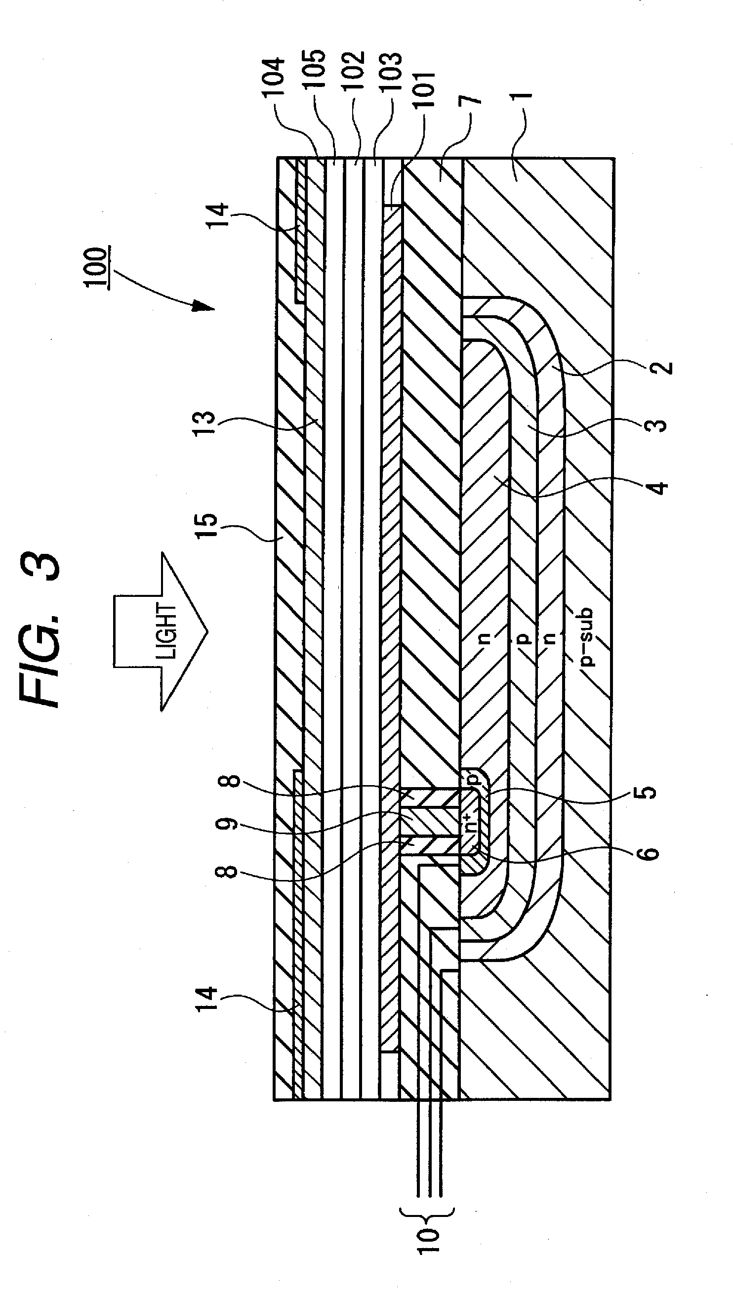
[0058]FIG. 3 is a fragmentary, schematic cross-section of a single pixel of a solid state imaging device 100 incorporating the second embodiment of the invention. Parts or members identified with the same numerals as in FIGS. 1 and 2 are identical.

[0059]The solid state imaging device 100 is composed of two-dimensionally arrayed pixels, one of which is illustrated in FIG. 3. One pixel outputs one signal that provides one pixel datum of image data.

[0060]The pixel of the solid state imaging device 100 shown in FIG. 3 includes a p type silicon substrate 1 and a photoelectric conversion element composed of a transparent insulating layer 7 formed on the p type silicon substrate, a lower electrode 101 formed on the insulating layer 7, a hole blocking layer 103 formed on the lower electrode 101, a photoelectric conversion layer 102 formed on the hole blocking layer 103, an electron blocking layer 105 formed on the photoelectric conversion layer 102, and an upper electr...

third embodiment

[III] Third Embodiment

[0068]The third embodiment provides a solid state imaging device of which each pixel is configured to detect two colors of light in a p type silicon substrate in which two photodiodes are not stacked in the substrate thickness direction as in FIG. 3 but arranged in a direction perpendicular to the direction of incident light.

[0069]FIG. 4 is a schematic cross-section of a single pixel of a solid state imaging device 200 incorporating the third embodiment. Parts or members identified with the same numerals as in FIGS. 1 and 2 are identical.

[0070]Each pixel of the solid state imaging device 200 illustrated in FIG. 4 includes a p type silicon substrate 17 and a photoelectric conversion element. The photoelectric conversion element is composed of a lower electrode 101 formed above the p type silicon substrate 17, a hole blocking layer 103 formed on the lower electrode 101, a photoelectric conversion layer 102 formed on the hole blocking layer 103, an electron blocki...


PUM


Abstract

A photoelectric conversion element includes a pair of electrodes, a photoelectric conversion layer provided between the pair of electrodes and a stress buffer layer provided between the photoelectric conversion layer and at least one of the electrodes, and the stress buffer layer has a stack structure comprising a crystalline sublayer.

Description

CROSS-REFERENCE TO RELATED APPLICATIONS[0001]This application claims the benefit of Japanese Patent Application JP 2008-161770, filed Jun. 20, 2008, the entire content of which is hereby incorporated by reference, the same as if set forth at length.FIELD OF THE INVENTION[0002]This invention relates to a photoelectric conversion element having a pair of electrodes and a photoelectric conversion layer therebetween and a solid-state imaging device having an array of a large number of the photoelectric conversion elements.BACKGROUND OF THE INVENTION[0003]A solid state imaging device having an array of photoelectric conversion elements is known, the photoelectric conversion element having a pair of electrodes and a photoelectric conversion layer of an organic or inorganic material between the electrodes.[0004]A photoelectric conversion element having an additional functional layer, such as a blocking layer (a carrier injection barrier to prevent dark current) or a crystallization prevent...

Claims


Application Information

Patent Timeline
Patent Type & Authority Applications(United States)
IPC IPC(8): H01L27/142
CPCH01L27/14623H01L27/14647H01L27/14692H01L27/305Y02E10/549H01L51/006H01L51/0065H01L51/4213H01L2251/308H01L51/0053H10K39/30H10K85/621H10K85/653H10K85/633H10K30/10H10K2102/103
Inventor HAYASHI, MASAYUKI
Owner FUJIFILM CORP
Why Eureka
Try Eureka