

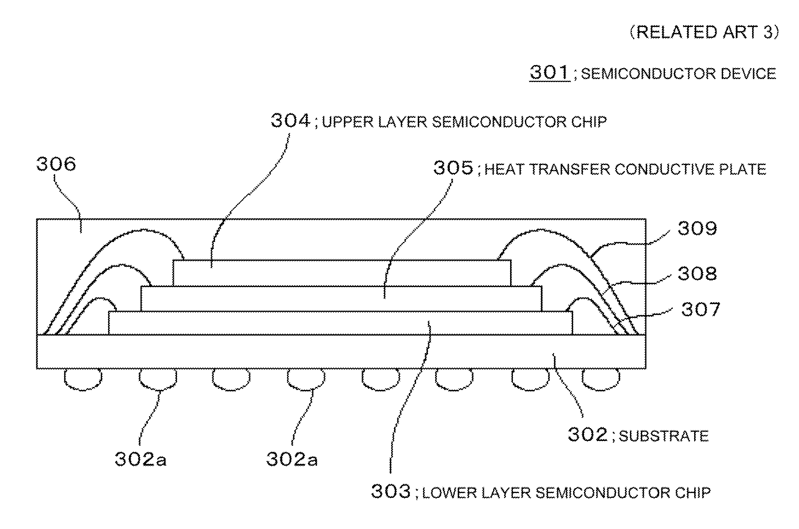
Semiconductor device
a technology of semiconductor devices and dielectric capacitors, applied in semiconductor devices, semiconductor/solid-state device details, electrical apparatus, etc., can solve the problems of noise generation of dc/dc converter circuits, noise generation through wires, and wiring is not considered, and achieves noise generation and noise generation. easy, high impedance, and easy to receive
- Summary
- Abstract
- Description
- Claims
- Application Information
AI Technical Summary
Benefits of technology
Problems solved by technology
Method used
Image

Examples
exemplary embodiment 1
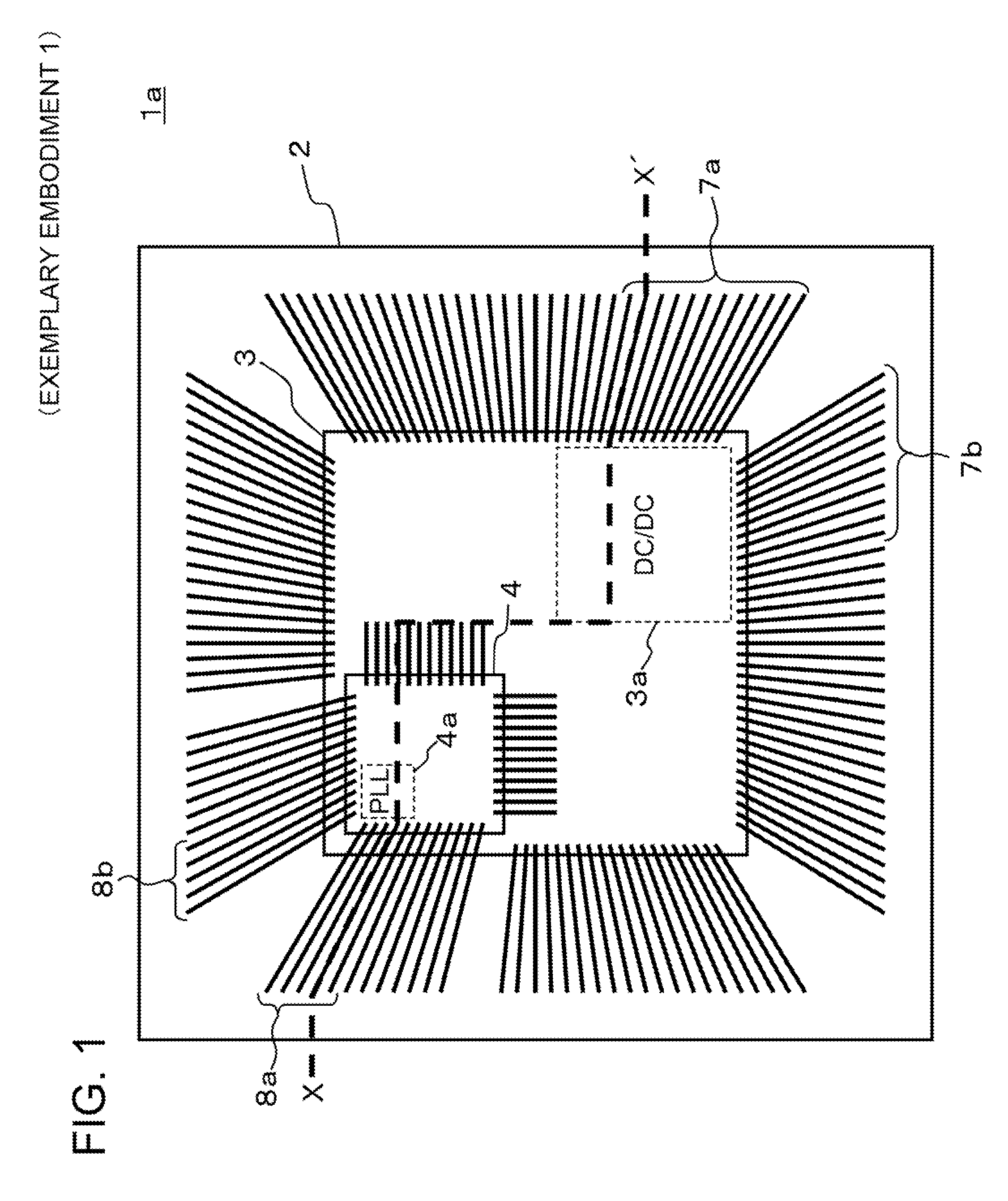
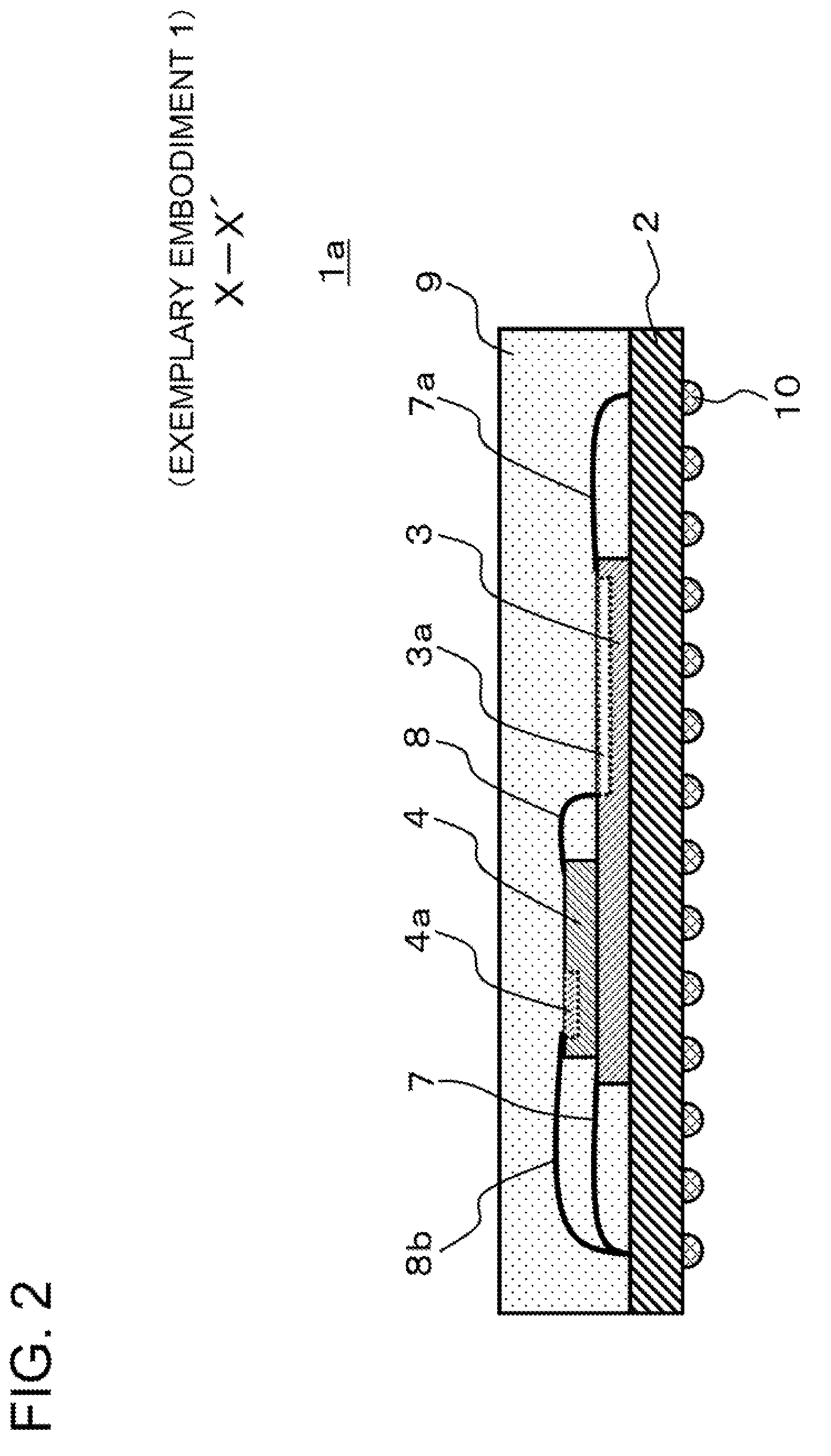
[0106]A semiconductor device according to exemplary embodiment 1 of the present invention is described using the drawings. FIG. 1 is a plan view schematically showing a configuration of the semiconductor device according to exemplary embodiment 1 of the present invention. FIG. 2 is a cross-sectional view of X-X′ in FIG. 1, schematically showing a configuration of the semiconductor device according to exemplary embodiment 1 of the present invention.
[0107]The semiconductor device 1a has a configuration in which a semiconductor chip 3 is stacked on a substrate 2, and a semiconductor chip 4 is stacked on the semiconductor chip 3. Wires for electrical connection (for example, 7a, 7b) are connected between the semiconductor chip 3 and the substrate 2. Wires for electrical connection (for example, 8a, 8b) are connected between the semiconductor chip 4 and the substrate 2. Wires for electrical connection are connected between the semiconductor chip 3 and the semiconductor chip 4.
[0108]The s...
exemplary embodiment 2
[0124]The semiconductor device according to exemplary embodiment 2 of the present invention is described using the drawings. FIG. 4 is a plan view schematically showing a configuration of the semiconductor device according to exemplary embodiment 2 of the present invention. FIG. 5 is a cross-sectional view taken along a line X-X′ in FIG. 4, schematically showing a configuration of the semiconductor device according to exemplary embodiment 2 of the present invention.
[0125]A semiconductor device 1b according to exemplary embodiment 2 differs from exemplary embodiment 1 in that an upper layer semiconductor chip 4 is stacked at approximately the center of a lower layer semiconductor chip 3, wires of the semiconductor chip 4 are laid out approximately in parallel at the top, bottom, left, and right of FIG. 4, and DC / DC converter circuits 3a, 3b, and 3c that generate noise are disposed at corners inside the lower layer semiconductor chip 3. According to this structure, the DC / DC converter...
exemplary embodiment 3
[0134]The semiconductor device according to exemplary embodiment 3 of the present invention is described using the drawings. FIG. 7 is a plan view schematically showing a configuration of the semiconductor device according to exemplary embodiment 3 of the present invention. FIG. 8 is a cross-sectional view taken along a line X-X′ in FIG. 7, schematically showing a configuration of the semiconductor device according to exemplary embodiment 3 of the present invention.
[0135]In exemplary embodiments 1 and 2, examples have been shown in which the upper layer semiconductor chip 4 is small in comparison to the lower layer semiconductor chip 3, but exemplary embodiment 3 has an example in which an upper layer semiconductor chip 4 is larger than a lower layer semiconductor chip 3. In this way, the upper layer semiconductor chip 4 is stacked at a place outside of a circuit (here, a DC / DC converter circuit) that generates noise inside the lower layer semiconductor chip 3, and a circuit (here, ...
PUM
 Abstract
Description
Claims
Application Information