Gallium nitride-based light emitting device with roughened surface and fabricating method thereof

Inactive Publication Date: 2009-12-31
ADVANCED OPTOELECTRONICS TECH
View PDF5 Cites 10 Cited by
  • Summary
  • Abstract
  • Description
  • Claims
  • Application Information

AI Technical Summary

Benefits of technology

[0015]According to the first preferred embodiment of the present invention, the doping concentration of magnesium into the heavily doped p-type III-nitride semiconductor layer is approximately 1021 to 1022 atoms per cubic centimeter so that a grown second p-type III-nitride semiconductor layer can have a characteristic of roughened surfaces.
[0016]The heavily doped p-type

Problems solved by technology

However, temperatures between 400 and 1000 degrees Celsius are lower than those used in other methods, and one disadvantage of using low temperatures to grow an aluminum indium gallium nitride layer is that the epitaxial quality is not easily controlled, and quantity of defects may increase so that the resistivity of the light emitting device may increase.
Generally, electrode pads are formed on the surface of a light emitting device and metallic wires are then bonded to the electrodes, and if the aluminum indium gallium nitride layer of the light emitting device is grown at relatively low temperatures, electron holes may not easily migrate through the aluminum indium galliu

Method used


Image

  • Gallium nitride-based light emitting device with roughened surface and fabricating method thereof
  • Gallium nitride-based light emitting device with roughened surface and fabricating method thereof

Examples


Embodiment Construction

[0021]One aspect of the present invention proposes a light emitting device. In order to provide a thorough understanding of the present invention, a detailed description of a number of method steps and components is provided below. Clearly, the practice of the present invention is not limited to any specific detail of a light emitting device that is familiar to one skilled in the art. On the other hand, components or method steps which are well-known are not described in detail to avoid unnecessary limitations. A preferred embodiment of the present invention will be described in detail. However, in addition to the preferred embodiment described, other embodiments can be broadly employed, and the scope of the present invention is not limited by any of the embodiments, but should be defined in accordance with the following claims and their equivalent.

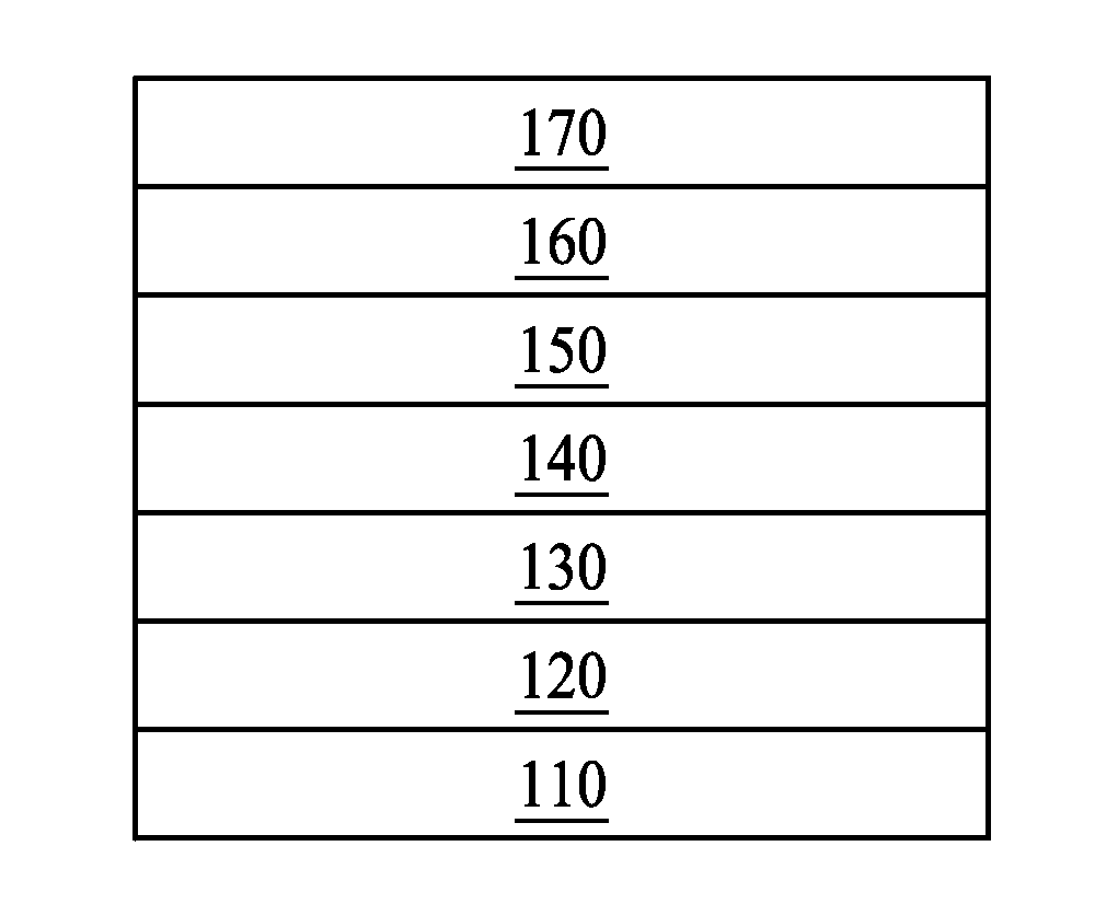
[0022]FIG. 1 is a sectional view showing a gallium nitride-based light emitting device with a roughened surface according to the first p...


PUM


Abstract

A gallium nitride-based light emitting device with a roughened surface is described. The light emitting device comprises a substrate, a buffer layer grown on the substrate, an n-type III-nitride semiconductor layer grown on the buffer layer, a III-nitride semiconductor active layer grown on the n-type III-nitride semiconductor layer, a first p-type III-nitride semiconductor layer grown on the III-nitride semiconductor active layer, a heavily doped p-type III semiconductor layer grown on the first p-type III-nitride semiconductor, and a roughened second p-type III-nitride semiconductor layer grown on the heavily doped p-type III semiconductor layer.

Description

BACKGROUND OF THE INVENTION[0001]1. Field of the Invention[0002]The present invention relates to an electronic product, and relates more particularly to a light emitting device.[0003]2. Description of the Related Art[0004]Generally, better light emitting devices are those that emit as much light as they can generate so as to provide maximum luminance and allow users to see more clearly.[0005]In order to increase luminance, some prior art technologies use roughened surfaces on light emitting devices. For example, U.S. Pat. No. 6,441,403 discloses a light emitting device of semiconductor, which uses a multiple quantum well structure to emit light. According to the specification of the patent, the method of fabricating the structure mainly grows an n-type (300) AlpInqGa1-p-qN layer or a p-type (100) aluminum indium gallium nitride layer at temperatures between 400 and 1000 degrees Celsius, with four elements (Aluminum, Indium, Gallium, and Nitrogen).[0006]The above-mentioned aluminum i...

Claims


Application Information

Patent Timeline
IPC IPC(8): H01L33/00H01L33/06H01L33/12H01L33/32
CPCH01L33/32H01L33/14
Inventor HUANG, SHIH CHENGTU, PO MINYEH, YING CHAOLIN, WEN YUWU, PENG YIHSU, CHIH PENGCHAN, SHIH HSIUNG
Owner ADVANCED OPTOELECTRONICS TECH
Why Eureka
Try Eureka