Multilayer ceramic electronic component and method for making the same

a technology of electronic components and ceramics, applied in the direction of variable capacitors, fixed capacitor details, fixed capacitors, etc., can solve the problems of difficult to ensure the quality of capacitors, the effect of limited amount of effective areas of internal conductors, and the likelihood of short circuit between internal conductors

Active Publication Date: 2009-12-31
MURATA MFG CO LTD
View PDF34 Cites 61 Cited by
  • Summary
  • Abstract
  • Description
  • Claims
  • Application Information

AI Technical Summary

Benefits of technology

[0011]To overcome the problems described above, preferred embodiments of the present invention provide a multilayer ceramic electronic component including

Problems solved by technology

Although further thickness reduction is currently being pursued, a problem arises in that short-circuits between internal conductors are more likely to occur with the thickness reduction of ceramic layers, thereby making it difficult to ensure the quality of the capacitors.
Thus, the amount by which the effective areas of the internal conductors can be increased is limited.
However, the amount by which the areas of the ceramic l

Method used


Image

  • Multilayer ceramic electronic component and method for making the same
  • Multilayer ceramic electronic component and method for making the same
  • Multilayer ceramic electronic component and method for making the same

Examples


Embodiment Construction

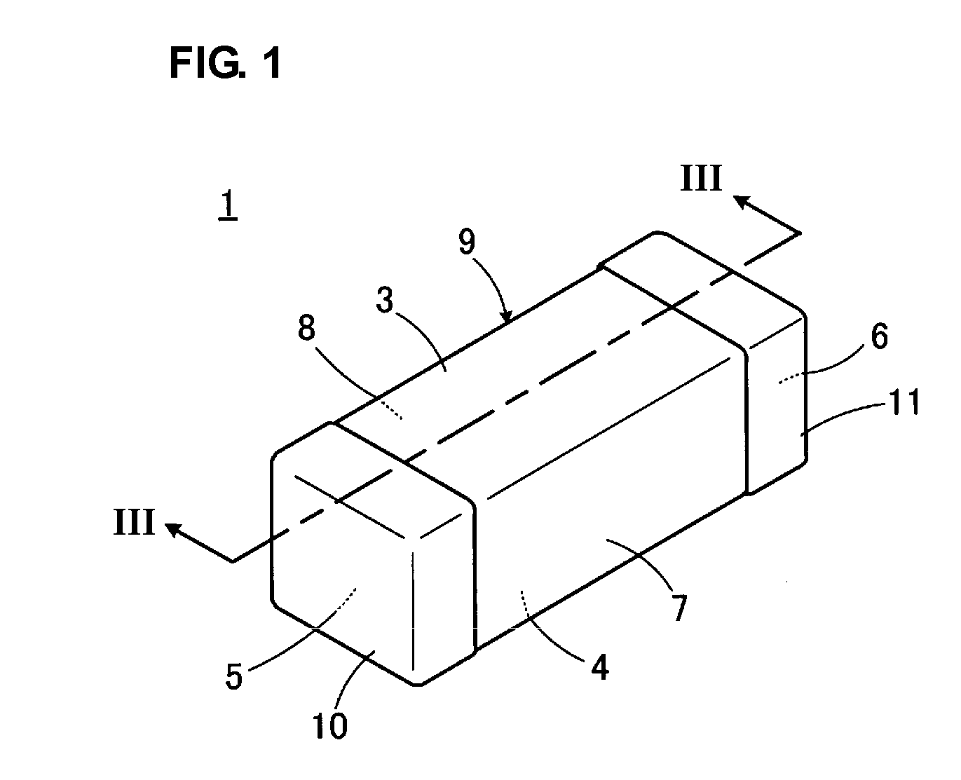
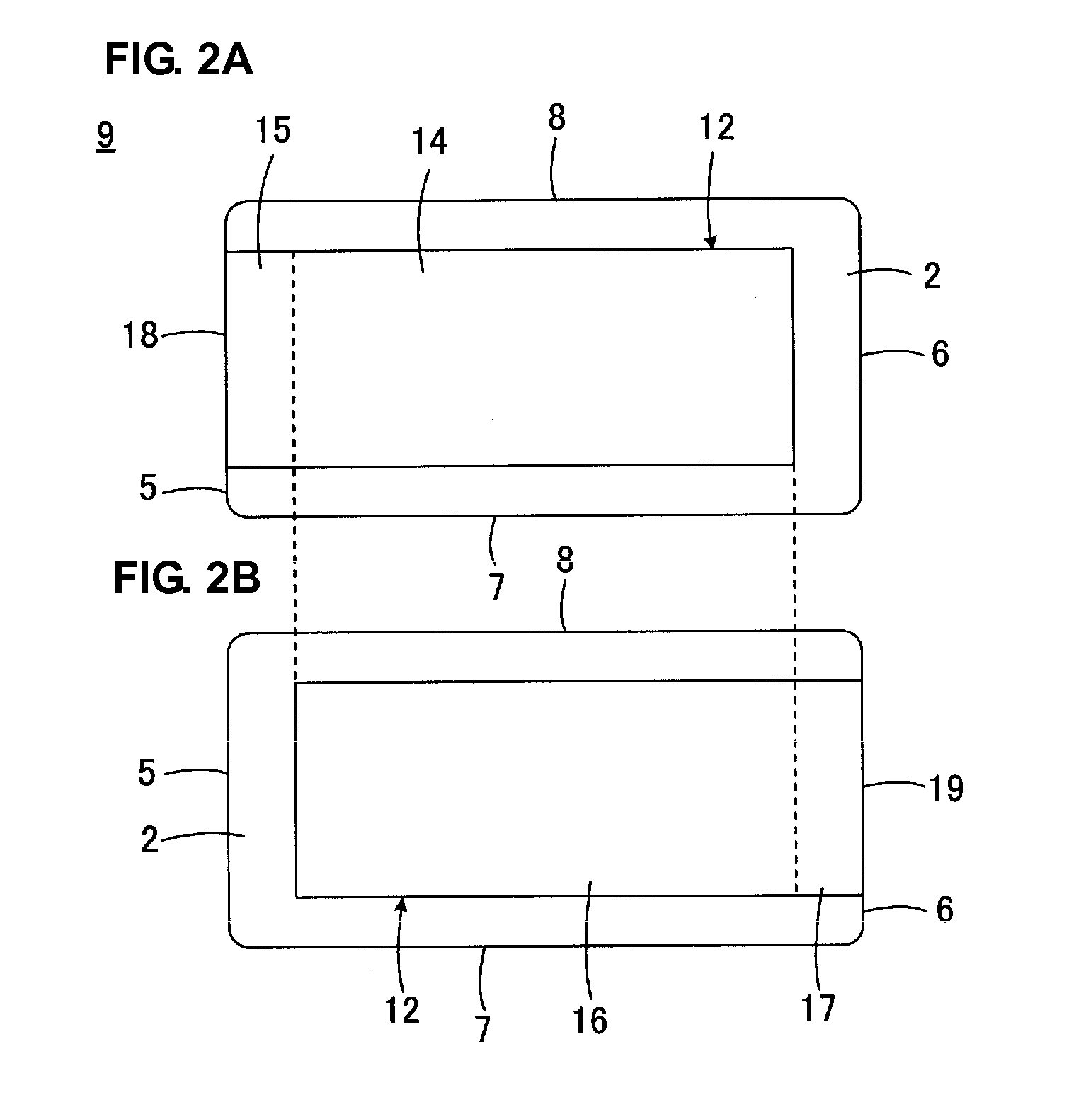
[0047]FIGS. 1 to 4 illustrate a first preferred embodiment of the present invention. FIG. 1 is a perspective view showing a multilayer ceramic electronic component 1. FIGS. 2A and 2B are plan views at two sections showing the internal structure of the multilayer ceramic electronic component 1 shown in FIG. 1. FIG. 3 is a cross-sectional view taken along line III-III in FIG. 1. FIG. 4 is an enlarged cross-sectional view showing a portion of FIG. 3.

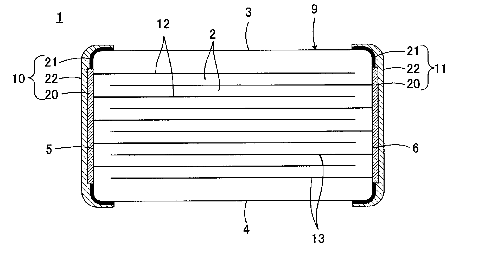
[0048]As shown in FIGS. 1 to 3, the multilayer ceramic electronic component 1 includes a ceramic body 9 defined by a plurality of stacked ceramic layers 2. The ceramic body 9 has a first main surface 3 and a second main surface 4 that faces the first main surface 3, and first to fourth side surfaces 5 to 8 that connect the first main surface 3 to the second main surface 4. The first side surface 5 faces the second side surface 6, and the third side surface 7 faces the fourth side surface 8.

[0049]A first external terminal electrode 10 is dis...


PUM

PropertyMeasurementUnit
Forceaaaaaaaaaa
Electrical conductoraaaaaaaaaa
Weightaaaaaaaaaa

Abstract

A multilayer ceramic electronic component includes external terminal electrodes that are formed by depositing metal plating films on exposed portions of internal conductors embedded in a ceramic body, depositing a copper plating films that cover the metal plating films and make contact with the ceramic body around the metal plating films, and heat-treating the ceramic body to generate a copper liquid phase, an oxygen liquid phase, and a copper solid phase between the copper plating films and the ceramic body. The mixed phase including these phases forms a region at which a copper oxide is present in a discontinuous manner inside the copper plating film at least at the interfaces between the ceramic body and the copper plating films. The copper oxide securely attaches the copper plating films to the ceramic body and enhances the bonding force of the external terminal electrodes.

Description

BACKGROUND OF THE INVENTION[0001]1. Field of the Invention[0002]The present invention relates to multilayer ceramic electronic components and methods for making the multilayer ceramic electronic components. In particular, the present invention relates to the structure of an external terminal electrode of a multilayer ceramic electronic component and a method for forming the external terminal electrode.[0003]2. Description of the Related Art[0004]In recent years, markets for small portable electronic appliances such as cellular phones, laptop computers, digital cameras, digital audio devices, etc., have expanded. These portable electronic appliances are achieving not only size reduction but also higher performance. Since a large number of multilayer ceramic electronic components are mounted on portable electronic appliances, multilayer ceramic electronic components are also required to achieve size reduction and higher performance. For example, multilayer ceramic capacitors are requi...

Claims


Application Information

Patent Timeline
IPC IPC(8): H01G4/30B05D5/12
CPCH01G4/005H01G4/232H01G4/30Y10T29/435
Inventor KOBAYASHI, TATSUNORIMOTOKI, AKIHIROOGAWA, MAKOTOIWANAGA, TOSHIYUKITAKEUCHI, SHUNSUKEKAWASAKI, KENICHI
Owner MURATA MFG CO LTD
Why Eureka
Try Eureka