Semiconductor device and manufacturing method therefor

a technology of semiconductor devices and manufacturing methods, applied in semiconductor devices, semiconductor/solid-state device details, electrical apparatus, etc., can solve the problems of reducing the spacing between wires, prone to electrical short circuit, and inability to bring close to chips, so as to suppress the bonding wire and prevent the bonding wire from colliding. , the effect of reducing the impact of the collision

Active Publication Date: 2010-01-07
RENESAS ELECTRONICS CORP
View PDF6 Cites 24 Cited by
  • Summary
  • Abstract
  • Description
  • Claims
  • Application Information

AI Technical Summary

Benefits of technology

[0009]The invention has been made based on the above findings of the present inventors. It is an object of the invention to provide a semiconductor device in which wires for coupling inner leads and a semiconductor chip with each other can be prevented from being electrically short-circuited to any other conductive part and a manufacturing method therefor.
[0011]In the semiconductor device in this embodiment, the upper face of the jutted portion of the power supply bar is positioned at a height lower than the upper faces of the tips of the inner lead portions. Therefore, even though a bonding wire at an inner lead portion collides with the power supply bar during the bonding thereof, the impact of the collision can be reduced. This makes it possible to suppress a bonding wire from being unintentionally bent (deformed) by the impact of the collision. As a result, it is possible to prevent a bonding wire for coupling an inner lead portion and a semiconductor chip from being electrically short-circuited to any other conductive part.

Problems solved by technology

In this case, the spacing between wires is reduced and leads are prone to be electrically short-circuited to one another.
Leads cannot be brought close to a chip to avoid this and because of a processing problem and this lengthens wires coupling a semiconductor chip and leads with each other.
The present inventors found the following problem arising when a power supply bar for supplying power to a semiconductor chip is extended to the area between a semiconductor chip and the tip of an inner lead: wires for coupling inner leads and the semiconductor chip with each other are lengthened and this makes it difficult to loop wires; and as a result, a wire collides with the power supply bar during the bonding thereof or any other like trouble occurs and the wire is electrically short-circuited to the power supply bar or other wires.

Method used


Image

  • Semiconductor device and manufacturing method therefor
  • Semiconductor device and manufacturing method therefor
  • Semiconductor device and manufacturing method therefor

Examples


first embodiment

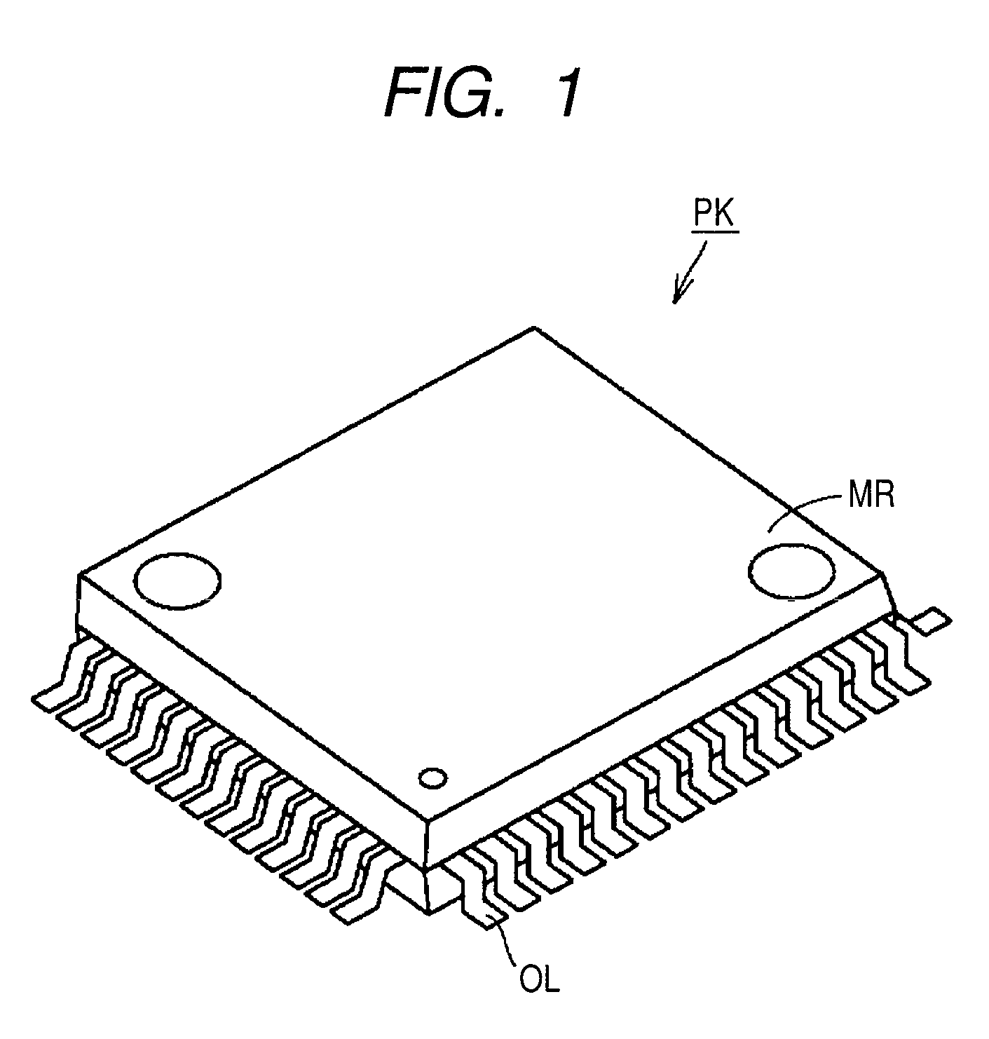
[0036]FIG. 1 is a perspective view schematically illustrating the configuration of a semiconductor device in the first embodiment of the invention. As illustrated in FIG. 1, the semiconductor device in this embodiment is a transfer mold type plastic package PK, for example, QFP (Quad Flat Package). In this type of package PK, outer lead portions OL are protruded from all the four sides on the circumference of sealing resin MR.

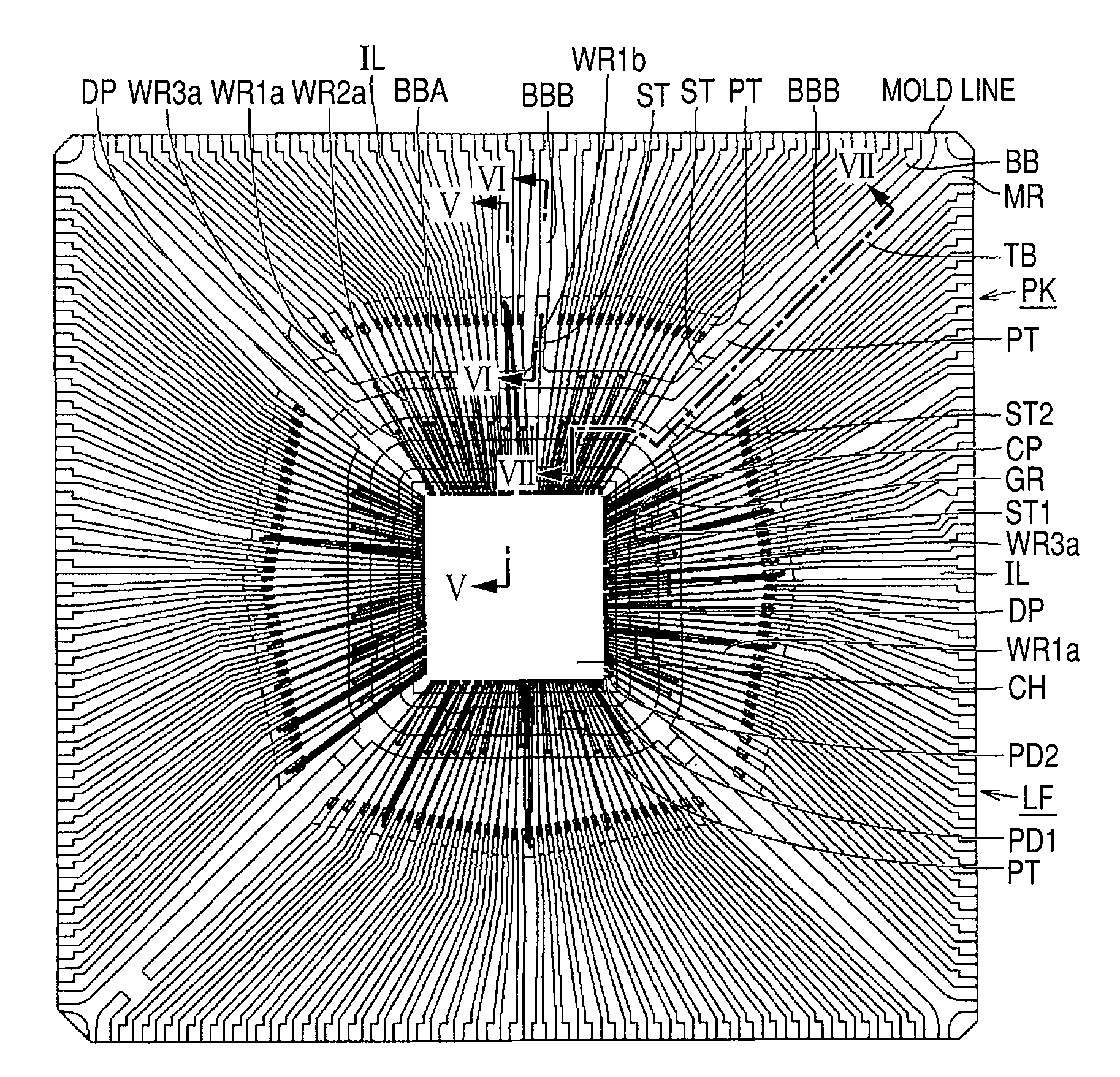
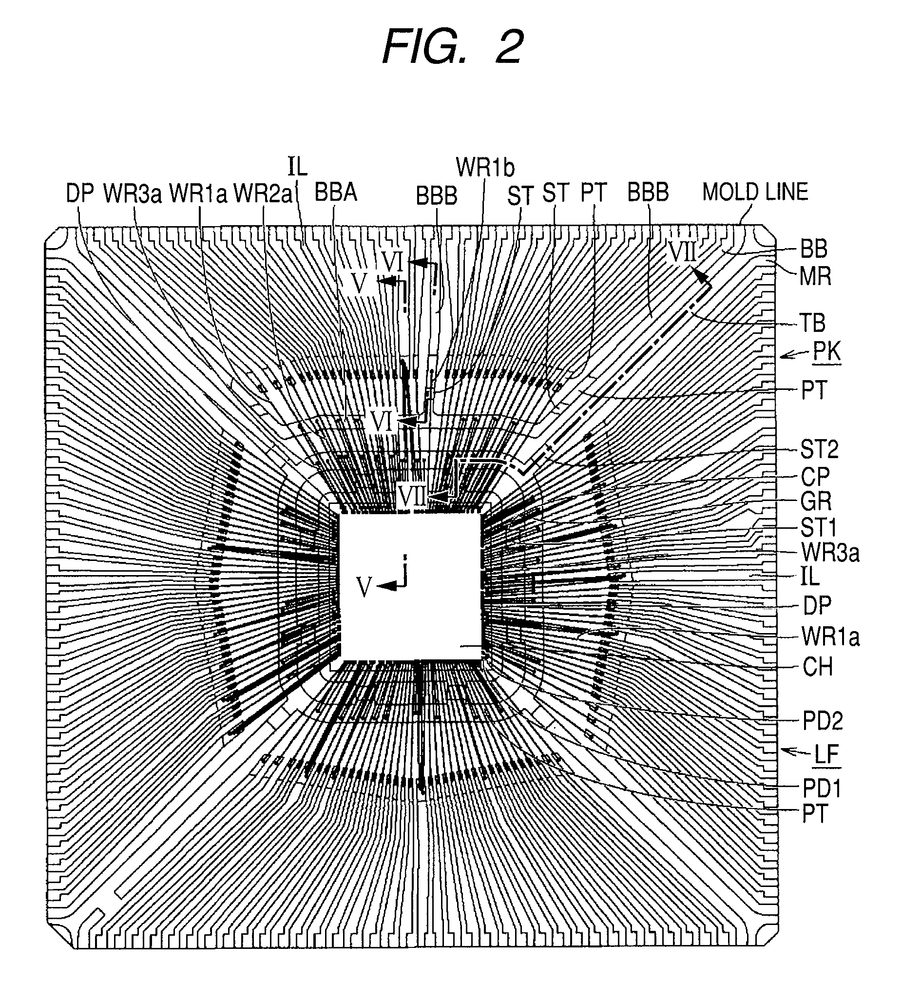
[0037]FIG. 2 is a schematic plan view illustrating the interior of the package PK illustrated in FIG. 1 as seen though the sealing resin. FIG. 3 is an enlarged view of FIG. 2 and in this drawing, bonding wires bonded to the inner lead portions are omitted. FIG. 4 is an enlarged view of FIG. 2 and in this drawing bonding wires bonded to the power supply bar or the GND ring are omitted. FIG. 5, FIG. 6, and FIG. 7 are schematic sectional views respectively taken along line V-V, line VI-VI, and line VII-VII of FIG. 2.

[0038]FIG. 6 illustrates a section of only the p...

second embodiment

[0079]FIG. 15 is a schematic plan view schematically illustrating the configuration of a semiconductor device in the second embodiment of the invention, illustrating the interior of the package as seen through sealing resin. FIG. 16 is a schematic sectional view taken along line XVI-XVI of FIG. 15. As illustrated in FIG. 15 and FIG. 16, for example, two semiconductor chips CH1, CH2, a lead frame LF, and bonding wires WR1a to WR3a, WR4, WR1b are arranged in the sealing resin MR in the package PK. The two semiconductor chips CH1, CH2 are stacked together.

[0080]In the upper face of the semiconductor chip CH1 positioned on the lower side, bonding pads PD1 to PD3 arranged in three rows along the outer edge are formed. Of the bonding pads in three rows of the semiconductor chip CH1, the bonding pads PD3 on the innermost row are electrically coupled with bonding pads PD4 of the semiconductor chip CH2 through bonding wires WR4.

[0081]As in the configuration in the first embodiment, the lead ...

third embodiment

[0102]FIG. 18 is a schematic plan view of the configuration of a semiconductor device in the third embodiment of the invention, illustrating an area in proximity to a parallel running portion of the power supply bar in FIG. 4 in closeup. In the configuration in this embodiment, as illustrated in FIG. 18, bonding wires WR1b are bonded not only to the jutted portion BBA of the power supply bar BB but also to a parallel running portion BBB. That is, a bonding wire WR1b is also bonded to a parallel running portion BBB sandwiched between two inner lead portions IL and extended in parallel with the adjoining inner lead portions.

[0103]In the description of this embodiment, the following case is taken as an example: a case where a bonding wire WR1b is bonded to the parallel running portion BBB coupled in the intermediate position, not at both ends, of the jutted portion BBA among the three parallel running portions BBB coupled to the jutted portion BBA. This bonding wire WR1b is bonded to t...


PUM


Abstract

A semiconductor device and a manufacturing method therefor wherein a wire for coupling an inner lead and a semiconductor chip with each other can be prevented from being electrically short-circuited to any other conductive part are provided. An inner lead portion has a tip arranged outside the outer circumferential end of the semiconductor chip as viewed on a plane. A power supply bar has a jutted portion extended between the outer circumferential end of the semiconductor chip and the tip of the inner lead portion as viewed on a plane. The upper face of the jutted portion is in a position lower than the upper face of the tip of the inner lead portion. A bonding wire for electrically coupling the semiconductor chip and the inner lead portion with each other has a bent portion outside the outer circumferential end of the semiconductor chip as viewed on a plane.

Description

CROSS-REFERENCE TO RELATED APPLICATIONS[0001]The disclosure of Japanese Patent Application No. 2008-172585 filed on Jul. 1, 2008 including the specification, drawings and abstract is incorporated herein by reference in its entirety.BACKGROUND OF THE INVENTION[0002]The present invention relates to semiconductor devices and manufacturing methods therefor and in particular to a semiconductor device having an inner lead portion electrically coupled with a semiconductor chip through a bonding wire and a manufacturing method therefor.[0003]When semiconductor packages are considered in terms of sealing structure, they are classified into two categories: hermetically sealed package and non-hermetically sealed package. Among non-hermetically sealed packages, especially, transfer mold type plastic packages are in the mainstream.[0004]This plastic package has such a structure that a semiconductor chip and leads are coupled with each other through wires and they are sealed with resin. This type...

Claims


Application Information

Patent Timeline
Patent Type & Authority Applications(United States)
IPC IPC(8): H01L23/495H01L21/60
CPCH01L21/565H01L2224/48599H01L23/4952H01L23/49541H01L23/49551H01L23/49582H01L24/06H01L24/45H01L24/49H01L24/78H01L24/85H01L2224/04042H01L2224/05553H01L2224/05599H01L2224/32245H01L2224/45144H01L2224/48091H01L2224/48095H01L2224/48137H01L2224/48247H01L2224/48253H01L2224/49052H01L2224/49109H01L2224/49113H01L2224/49171H01L2224/49175H01L2224/49431H01L2224/73265H01L2224/78301H01L2224/85181H01L2224/85399H01L2924/01004H01L2924/01005H01L2924/01014H01L2924/0102H01L2924/01046H01L2924/01073H01L2924/01078H01L2924/01079H01L2924/01082H01L24/48H01L2924/01006H01L2924/01023H01L2924/01033H01L2924/01065H01L2924/00014H01L23/3107H01L2924/00H01L2224/05554H01L2224/45015H01L2924/181H01L2224/49433H01L2924/00012
Inventor MISUMI, KAZUYUKIFUKUDOME, KATSUYUKIHATAUCHI, KAZUSHIFUKUHARA, KAZUYAYAMASHITA, KUNIHIRO
Owner RENESAS ELECTRONICS CORP
Why Eureka
Try Eureka