Display device and method of manufacturing the same

a technology of display device and manufacturing method, which is applied in the direction of printed circuit stress/warp reduction, electrical apparatus casing/cabinet/drawer, instruments, etc., can solve the problems of display unevenness, display distorted, unevenness greatly affecting the display image, etc., and achieve the effect of suppressing the occurrence of display unevenness without increasing the panel size and the number of parts

Inactive Publication Date: 2010-01-07
NEC LCD TECH CORP
View PDF2 Cites 12 Cited by
  • Summary
  • Abstract
  • Description
  • Claims
  • Application Information

AI Technical Summary

Benefits of technology

[0020]An exemplary object of the present invention is to provide a display device and its manufacturing method which enables to suppress the occurrence of the display unevenness without increasing panel size and the number of parts by surely absorbing the stress due to the thermal deformation of the drive circuit component.

Problems solved by technology

Because of this, the glass substrate is tended to be distorted greatly, and thus a display unevenness caused by deformation of the glass substrate occurs remarkably compared with the other installation methods.
Particularly, the display unevenness greatly affects a display image when the image is darkly displayed.
However, in the above-mentioned IC chip mounting method, when the IC chip 4 is thermal-compressed, there a problem that the IC chip 4 warps in a concave shape due to thermal expansion difference between the IC chip 4 and the glass substrate (the TFT substrate 2).
As a result, the thickness of the liquid crystal layer changes locally by this distorted deformation, and the display unevenness (150) occurs at the display area nearby the IC chip mounting area owing to double refraction occurred in the glass substrate, and thereby aggravating the display quality.
At that time, the wider the interval between adjacent IC chips 4, the larger the amplitude of the distorted deformation, and thus the shade of the display unevenness becomes worse.
However, when the IC chip is heated and pressurized by the compression bonding tool from the face opposite to the active face of the IC chip in the compressing step of the IC chip, because the slit is provided on the interface with the compression bonding tool in the patent document 1, the projected electrode member arranged on the active face opposing to the slit portion does not receive the pressure, and thereby tending to cause such problem as connection fault.
First, because the space is needed for providing the deformation suppression members, larger area is needed for mounting components, and results in disadvantageous for the miniaturization of the display device.
Second, because the deformation supression members and its bonding material are needed for the problem solution, number of parts are increased and increase in weight is inevitable for the display device where the weight saving is required.

Method used


Image

  • Display device and method of manufacturing the same
  • Display device and method of manufacturing the same
  • Display device and method of manufacturing the same

Examples


exemplary embodiment 1

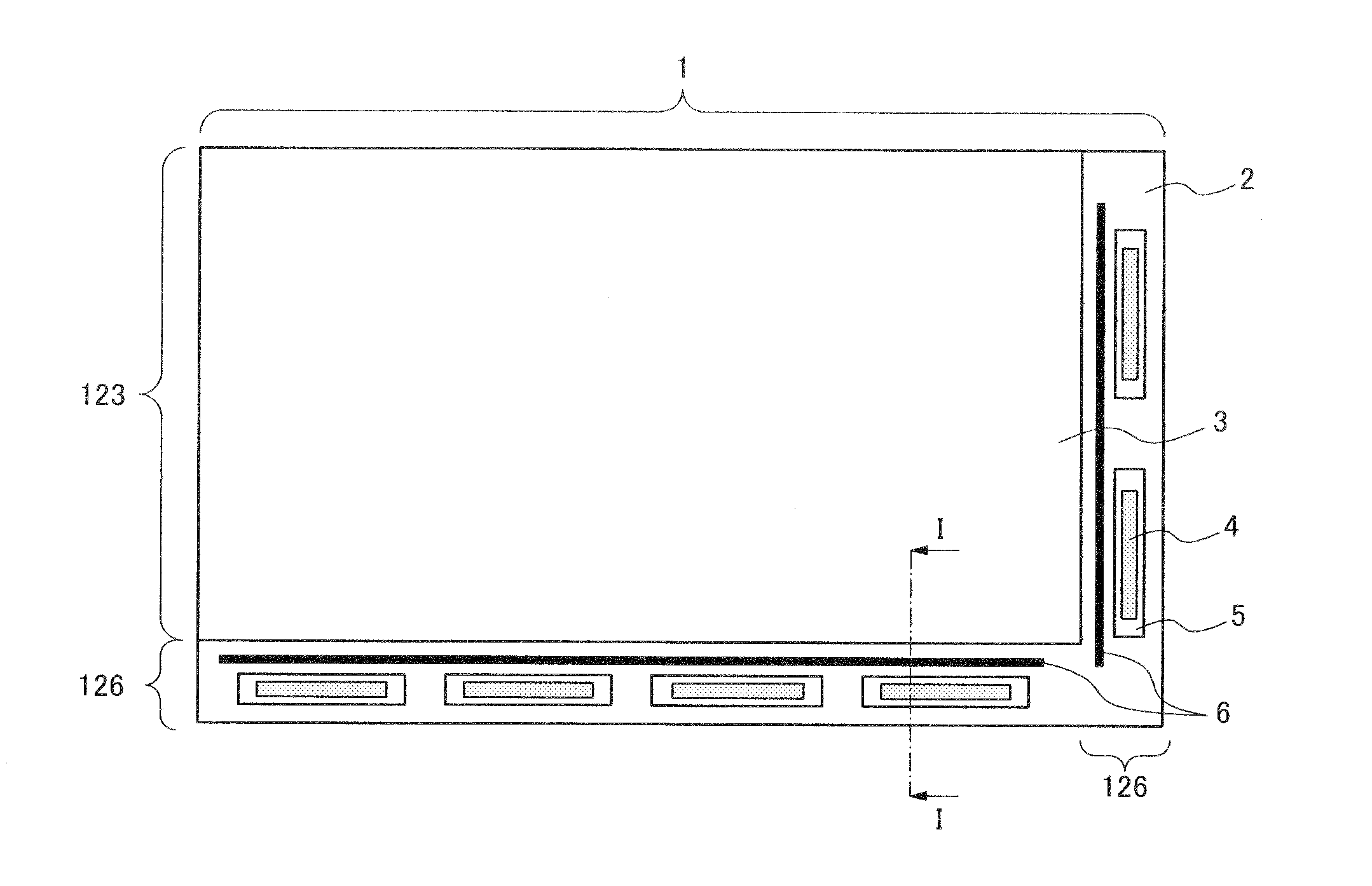
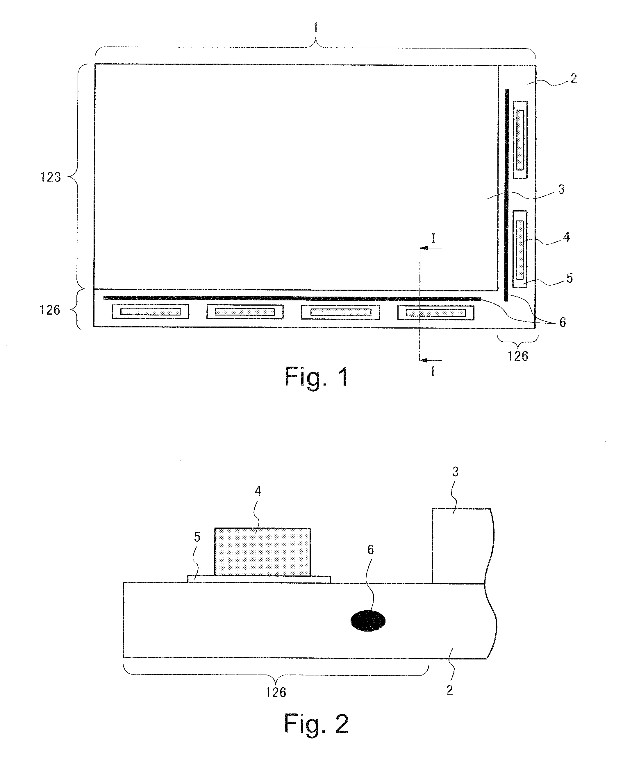
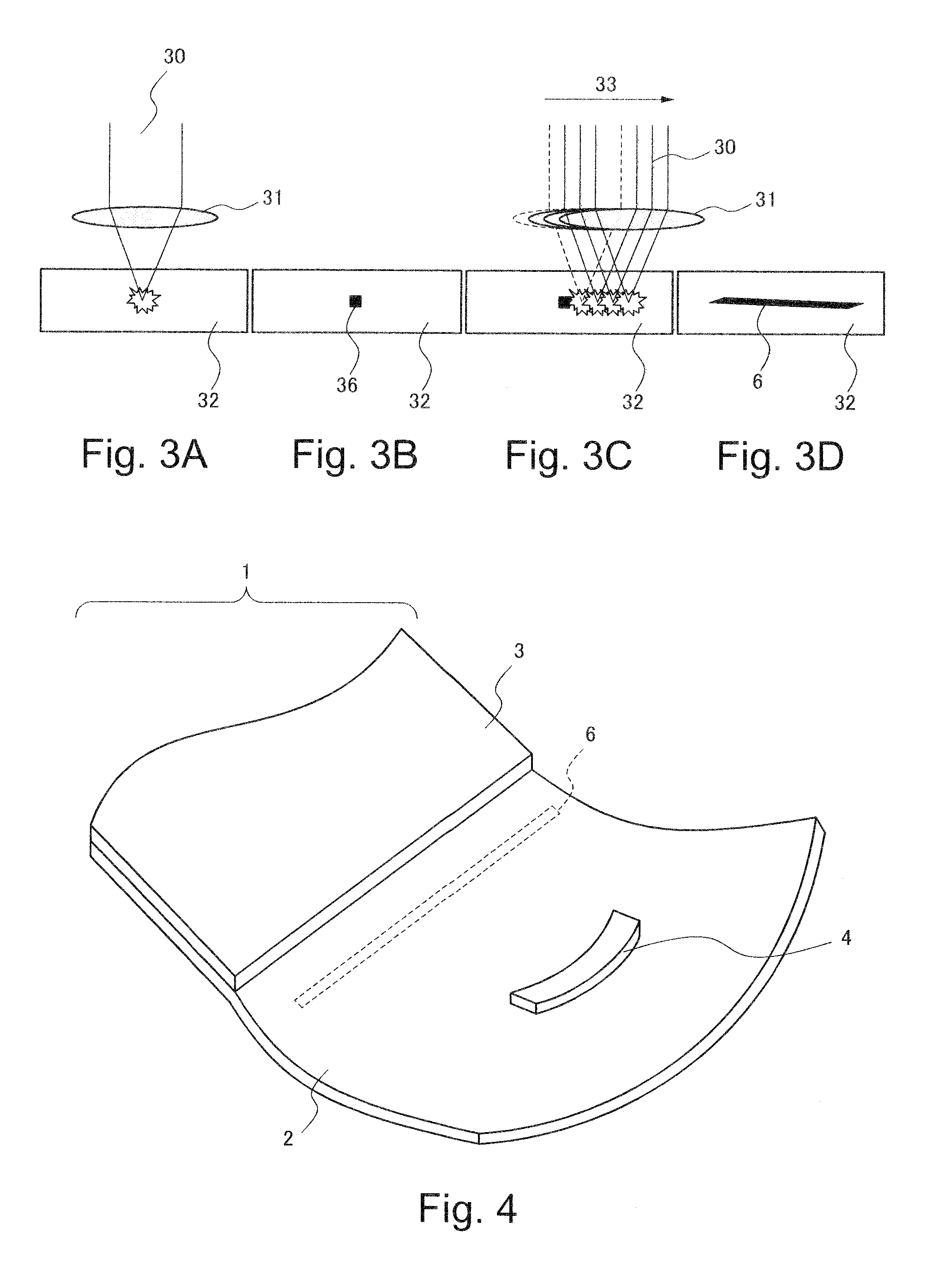
[0046]First, a display device according to the first exemplary embodiment of the present invention will be described with reference to FIG. 1 through FIG. 5. FIG. 1 is a plan view showing a structure of a display panel according to the first exemplary embodiment of the present invention, and FIG. 2 is a cross sectional view along the I-I line shown in FIG. 1. FIG. 3A through FIG. 3D are cross sections showing forming processes of the stress absorption regions of this exemplary embodiment, and FIG. 4 is a perspective view showing the state after mounting an IC chip on the display panel of this exemplary embodiment. FIG. 5 is a plan view showing the other structure of the display panel according to this exemplary embodiment.

[0047]As shown in FIG. 1, a display panel 1 of this exemplary embodiment includes two glass substrates each having thickness in the order of 0.7 mm, one of which is a thin film transistor substrate (hereinafter, abbreviated as a TFT substrate 2) provided with trans...

exemplary embodiment 2

[0064]Next, a display device according to a second exemplary embodiment of the present invention will be described with reference to FIG. 6 through FIG. 11. Among those figures, FIG. 6A, FIG. 7A and FIG. 8A are plan views showing the structures of the display panel related to the second exemplary embodiment of the present invention, and FIG. 6B, FIG. 7B and FIG. 8B are partial expanded plan views corresponding to respective dotted line section in FIG. 6A, FIG. 7A and FIG. 8A. FIG. 9A is a plan view showing the other structure of the display panel according to the second exemplary embodiment and FIG. 9B is a cross sectional view along the II-II line shown in FIG. 9A. FIG. 10 is a cross sectional view along the III-III line of FIG. 9A. FIGS. 11A to 11D are plan views showing additional other structures of the display panels according to this exemplary embodiment. This exemplary embodiment is achieved by revising the shape of the stress absorption regions of the first exemplary embodim...


PUM

PropertyMeasurementUnit
thicknessaaaaaaaaaa
thicknessaaaaaaaaaa
widthaaaaaaaaaa

Abstract

A display device includes a glass substrate having a display area and a peripheral area. A drive circuit component is mounted on the glass substrate by thermocompression bonding on the peripheral area, and a stress absorption region is provided within the glass substrate close to the circuit component so as to absorb stress produced by thermal deformation of the circuit component. A method of manufacturing the display device of the present invention includes a step of forming stress absorption region into the glass substrate so as to absorb the stress caused by thermocompression bonding of the the circuit component.

Description

[0001]This application is based upon and claims the benefit of priority from Japanese patent application No. 2008-175273, filed on Jul. 4, 2008 and the disclosure of which is incorporated herein in its entirety by reference.TECHNICAL FIELD[0002]The present invention relates to a display device and its manufacturing method, and more particularly to the display device and its manufacturing method having a glass substrate on which a drive circuit component is mounted by using a thermocompression bonding.BACKGROUND ART[0003]As an example of display devices, a liquid crystal display (LCD) device is widely used in industrial applications, and in recent years, a new market has been growing as display monitors in broadcasting stations and medical imaging devices. When using it at the place with very dark operating environment like the above-mentioned display monitors in the broadcasting stations, a slight brightness difference in a display screen is visually recognized remarkably compared w...

Claims


Application Information

Patent Timeline
Patent Type & Authority Applications(United States)
IPC IPC(8): H05K5/00H05K3/20
CPCG02F1/13452H05K1/0271Y10T29/49128H05K1/0306H05K1/0272
Inventor FUJITA, AKIRAKONDO, YUJI
Owner NEC LCD TECH CORP
Why Eureka
Try Eureka