Design layout data creating method, computer program product, and method of manufacturing semiconductor device
a technology of layout data and creating method, which is applied in the direction of cad circuit design, total factory control, instruments, etc., can solve the problems of affecting the shape of the pattern on the wafer, the influence of diffraction of exposing light on the dimensions on the wafer, and the difficulty of mask manufacturing and the wafer process for accurately forming fine patterns,
- Summary
- Abstract
- Description
- Claims
- Application Information
AI Technical Summary
Problems solved by technology
Method used
Image


Examples
Embodiment Construction
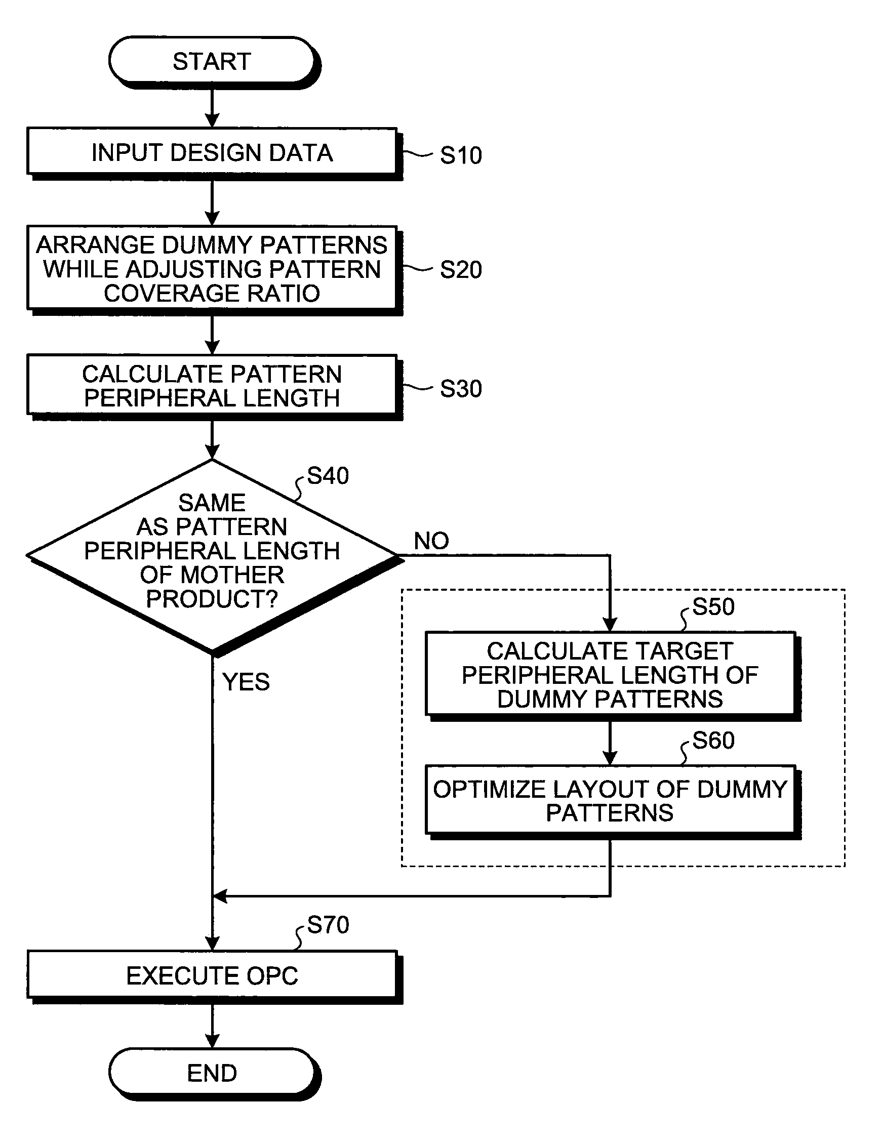
[0021]Exemplary embodiments of the present invention are explained in detail below. The present invention is not limited by the embodiments.
[0022]FIG. 1 is a diagram of a configuration of a mask data creating apparatus according to an embodiment of the present invention. A mask data creating apparatus 100 is an apparatus such as a computer that creates design layout data (design data) and mask pattern data of a photomask used for exposure processing of a semiconductor device manufacturing process. The mask data creating apparatus 100 includes a central processing unit (CPU) 1, a read only memory (ROM) 2, a random access memory (RAM) 3, a display unit 4, and an input unit 5. In the mask data creating apparatus 100, the CPU 1, the ROM 2, the RAM 3, the display unit 4, and the input unit 5 are connected via a bus line.
[0023]The CPU 1 creates design layout data using a layout data creation program (a pattern design program) 7, which is a computer program for designing design layout data...
PUM
 Abstract
Description
Claims
Application Information