Lateral Double Diffused Metal Oxide Semiconductor (LDMOS) Device and Method of Manufacturing LDMOS Device

a metal oxide semiconductor and lateral double-diffusive technology, applied in the direction of semiconductor devices, basic electric elements, electrical apparatus, etc., can solve the problems of surface breakdown and less than optimal current drive capability, and achieve the effect of increasing the breakdown voltage and reducing the on-resistance of the devi

Inactive Publication Date: 2010-01-14
COLUMBA TECH INC
View PDF3 Cites 71 Cited by
  • Summary
  • Abstract
  • Description
  • Claims
  • Application Information

AI Technical Summary

Benefits of technology

[0013]An object of the present invention is to provide an LDMOS device capable of increasing a breakdown voltage while reducing an on-res

Problems solved by technology

Accordingly, the current drive capability may be less than optimal.
Therefore

Method used


Image

  • Lateral Double Diffused Metal Oxide Semiconductor (LDMOS) Device and Method of Manufacturing LDMOS Device
  • Lateral Double Diffused Metal Oxide Semiconductor (LDMOS) Device and Method of Manufacturing LDMOS Device
  • Lateral Double Diffused Metal Oxide Semiconductor (LDMOS) Device and Method of Manufacturing LDMOS Device

Examples


Embodiment Construction

[0027]Reference will now be made in detail to a lateral double diffused metal oxide semiconductor (LDMOS) device according to exemplary embodiment(s) of the present invention, examples of which are illustrated in the accompanying drawings. Wherever possible, the same reference numbers will be used throughout the drawings to refer to the same or like parts.

[0028]In the following description, only features directly related to the invention will be explained while omitting description about well-known functions, structures, and components so as not to obscure the present invention.

[0029]It will be understood that when an element such as a layer, region, pattern or structure is referred to as being “on” or “under” another element, the element may be disposed “directly” on another element or “indirectly” by having one or more interposing elements between them.

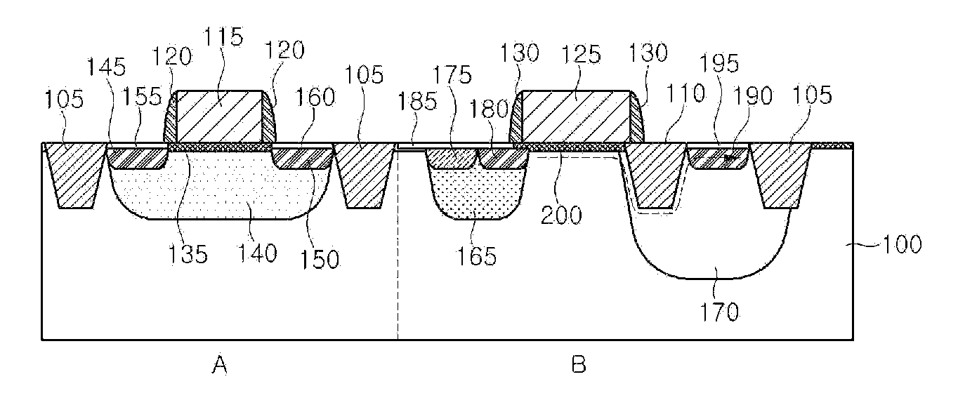
[0030]Referring to FIG. 8, the LDMOS device according to an embodiment of the present invention includes a low voltage MOS (LV MOS...


PUM


Abstract

A method for manufacturing a lateral double diffused metal oxide semiconductor (LDMOS) device includes forming an oxide layer on a semiconductor substrate, forming first and second trenches by partially etching the oxide layer and the semiconductor substrate, forming a small trench overlapping with the second trench so that the second trench has a stepped structure, and depositing one or more dielectric layers so that the first trench forms a device isolation layer defining a semiconductor device region and the second trench having a stepped structure forms a drain extension device isolation layer. The breakdown voltage of the LDMOS device may be improved while reducing the on-resistance, thereby improving the operational reliability of the device.

Description

[0001]This application claims the benefit of the Korean Patent Application No. 10-2008-0066539, filed on 9 Jul. 2008, which is hereby incorporated by reference as if fully set forth herein.BACKGROUND OF THE INVENTION[0002]1. Field of the Invention[0003]The present invention relates to a lateral double diffused metal oxide semiconductor (LDMOS) device and a manufacturing method for the same.[0004]2. Discussion of the Related Art[0005]A lateral double diffused metal oxide semiconductor (LDMOS) is a sort of majority carrier device and also a representative of lateral type power device having quick switching responsiveness and high input impedance.[0006]FIG. 1 is a cross-sectional view showing the structure of a conventional LDMOS device. Referring to the drawing, a semiconductor substrate 100 is divided by a device isolation layer 105 into a low voltage MOS (LV MOS) region A disposed on the left, and a high voltage MOS (HV MOS) region B disposed on the right.[0007]The LV MOS region A a...

Claims


Application Information

Patent Timeline
IPC IPC(8): H01L29/78H01L21/336H01L21/762
CPCH01L21/823807H01L21/823814H01L29/7835H01L29/0653H01L29/66659H01L21/823878H01L21/76H01L21/18
Inventor LEE, YONG JUN
Owner COLUMBA TECH INC
Why Eureka
Try Eureka