Switching control circuit, semiconductor device and switching power source apparatus

a control circuit and switching power technology, applied in the direction of electric variable regulation, process and machine control, instruments, etc., can solve the problems of power source cannot be started, energy required to raise the output voltage voutp to a predetermined voltage, etc., to achieve shorten the on period, suppress current, and reduce the effect of power consumption

Inactive Publication Date: 2010-01-14
COLLABO INNOVATIONS INC
View PDF8 Cites 33 Cited by
  • Summary
  • Abstract
  • Description
  • Claims
  • Application Information

AI Technical Summary

Benefits of technology

[0044]With the switching control circuit, the semiconductor device and the switching power source apparatus according to the present invention, at the starting time and an overload time in which the output voltage of the switching power source apparatus is low, if an overcurrent state, in which the ON period of the switching device becomes short and a current not less than the current limit value of the switching device flows through the switching device, occurs, this overcurrent state is detected. The nullification period is made shorter than the nullification period that is obtained during steady operation, and the ON period of the switching device is made short. Hence, the current flowing through the switching device can be made small in each pulse for the switching operation, and, at the same time, the current can be suppressed from increasing each time a pulse for the switching operation is generated. For this reason, the overcurrent state of the switching device can be resolved, and degradation of and damage to the switching device due to the flow of the device current not less than the allowable current value can be prevented.
[0045]In addition, in the case that the inclination of the waveform of the current flowing through the switching device is large, that is, in the case that the rate of increase in the current in each pulse for the switching operation is high, and even in the case that the output voltage is limitlessly close to zero and the energy stored in the switching transformer hardly decreases in the OFF period of the switching device, protection is activated to shorten the ON period in each pulse for the switching operation. Hence, the current in each pulse for the switching operation can be made small, and the increase in the current in each pulse for the switching operation can be suppressed. As a result, the switching device can be prevented from being degraded and damaged.
[0046]Furthermore, even in the case that the characteristics of the components inside the switching power source apparatus have changed due to variations and temperature characteristics of the components, protection is activated to shorten the ON period in each pulse for the switching operation. As a result, the effect hardly decreases, and the reliability of the switching power source apparatus can be improved.
[0047]Moreover, the switching device and the control circuit can be provided inside one semiconductor chip and formed into a monolithic IC easily. As described above, by providing the main circuit components inside one semiconductor chip, the number of components constituting the circuit can be reduced. Hence, a switching control circuit serving as a power source apparatus can be made smaller in size, lighter in weight and lower in cost easily.

Problems solved by technology

However, the overcurrent protection methods in the conventional switching control circuits have the following problems.
However, if the frequency of the switching operation is lowered excessively, energy required to raise the output voltage VOUTp to a predetermined voltage is not obtained, for example, at the starting time, and another problem, that is, a faulty starting state in which the power source cannot be started, occurs.

Method used


Image

  • Switching control circuit, semiconductor device and switching power source apparatus
  • Switching control circuit, semiconductor device and switching power source apparatus
  • Switching control circuit, semiconductor device and switching power source apparatus

Examples


embodiment 1

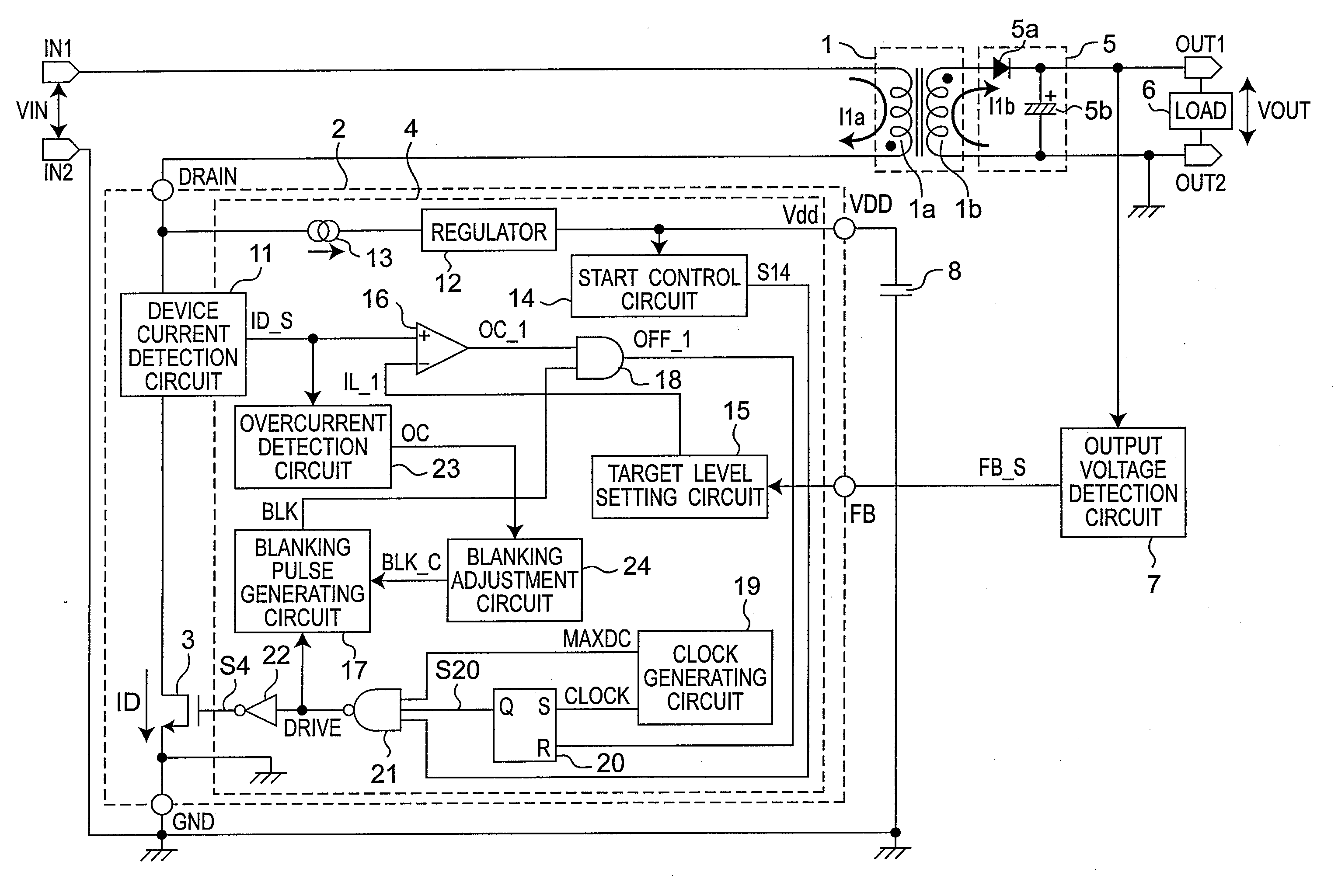
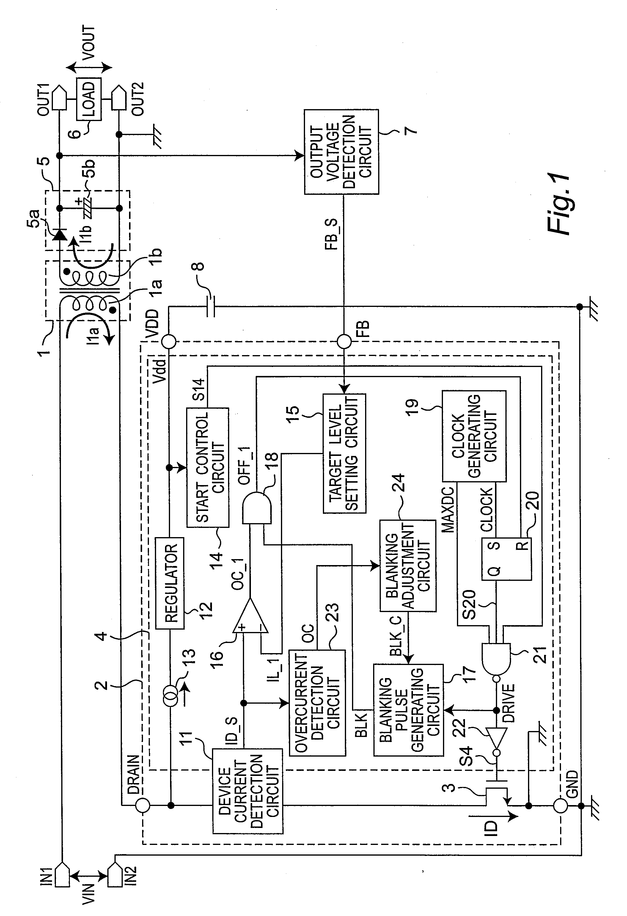
[0073]FIG. 1 is a block diagram showing a configuration example of a switching power source apparatus according to Embodiment 1.

[0074]This switching power source apparatus is configured by using the current mode PWM (pulse-width modulation) control method as a method for controlling the switching operation of a switching device.

[0075]In FIG. 1, the switching power source apparatus contains an input terminal IN1, an input terminal IN2, an output terminal OUT1, an output terminal OUT2, a switching transformer 1, an output voltage generating circuit 5, an output voltage detection circuit 7, a capacitor 8, and a switching control circuit 2. The switching power source apparatus supplies a substantially DC output voltage VOUT to a load 6 connected across the output terminals OUT1 and OUT2 on the basis of a substantially DC input voltage VIN input across the input terminals IN1 and IN2. The switching control circuit 2 contains a switching device 3, a drain terminal DRAIN, an internal circu...

embodiment 2

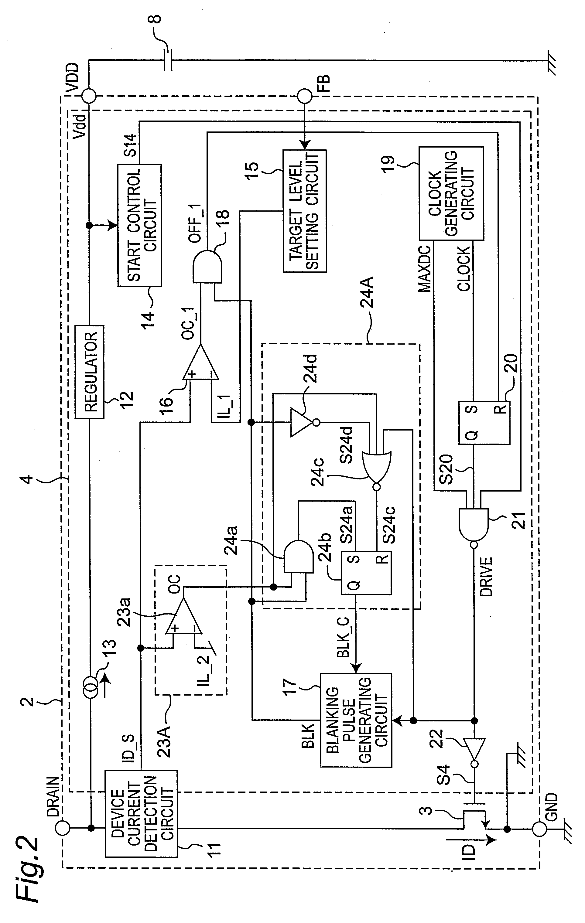
[0137]In the following description of Embodiment 2, differences from Embodiment 1 will be mainly described. Since the configurations, operations and effects other than those relating to the differences are similar to those according to Embodiment 1, their descriptions are omitted.

[0138]FIG. 7 is a block diagram showing a configuration example of a switching control circuit according to Embodiment 2. In FIG. 7, a control circuit 4a differs from the control circuit 4 according to Embodiment 1 in that a blanking adjustment circuit 24B inside the control circuit 4a contains a comparison circuit 24e for overcurrent resolution and that the three-input NOR circuit 24c uses the output signal of the comparison circuit 24e for overcurrent resolution instead of the overcurrent detection signal OC.

[0139]The comparison circuit 24e for overcurrent resolution compares the level of the device current detection signal ID_S with a limit level IL_3 lower than the limit level IL_2 and generates a compa...

embodiment 3

[0147]In the following description of Embodiment 3, differences from Embodiments 1 and 2 will be mainly described. Since the configurations, operations and effects other than those relating to the differences are similar to those according to Embodiments 1 and 2, their descriptions are omitted.

[0148]FIG. 9 is a block diagram showing a configuration example of a switching control circuit according to Embodiment 3. In FIG. 9, the configuration of a control circuit 4b differs from those of the control circuits according to Embodiment 1 and 2 in that a blanking adjustment circuit 24C inside the control circuit 4b contains an AND circuit 24g and a counting circuit 24f for overcurrent resolution and that the AND circuit 24g and the counting circuit 24f for overcurrent resolution are used to reset the flip-flop circuit 24b.

[0149]In the AND circuit 24g, the logical AND signal S24g thereof becomes high when both the adjustment signal BLK_C and the clock signal CLOCK are high, and becomes lo...


PUM


Abstract

At the starting time and an overload time in which the output voltage of the switching power source apparatus is low, if an overcurrent state, in which the ON period of the switching device becomes short and a current not less than the current limit value of the switching device flows through the switching device, occurs, this overcurrent state is detected. The blanking period of a blanking pulse signal is made shorter than the blanking period that is obtained during steady operation, and the ON period of the switching device is made shorter. Hence, the device current flowing through the switching device can be made small in each pulse for the switching operation, and, at the same time, the device current is suppressed from increasing each time a pulse for the switching operation is generated.

Description

[0001]The disclosure of Japanese Patent Application No. 2008-178698 filed Jul. 9, 2008 including specification, drawings and claims is incorporated herein by reference in its entirety.BACKGROUND OF THE INVENTION[0002]1. Field of Invention[0003]The present invention relates to a switching control circuit, a semiconductor device and a switching power source apparatus having an overcurrent protection function for protecting a switching device.[0004]2. Description of Related Art[0005]In a switching power source apparatus for supplying a stable DC voltage to a load, current limitation is generally provided to prevent a current having a predetermined value or more from flowing through a switching device. However, at the starting time and an overload time in which the output voltage of the switching power source apparatus is low, the current having the predetermined value or more flows through the switching device, that is, the so-called overcurrent state of the switching device occurs, an...

Claims


Application Information

Patent Timeline
Patent Type & Authority Applications(United States)
IPC IPC(8): H02M3/335H02H7/122H02M7/44
CPCH02M2001/0038H02M3/33507H02M1/0038
Inventor KAWABE, KEITAMURATA, KAZUHIROMORI, YOSHIHIROMOROTA, NAOHIKO
Owner COLLABO INNOVATIONS INC
Why Eureka
Try Eureka