Nanowire photovoltaic cells and manufacture method thereof

a photovoltaic cell and nanowire technology, applied in the field of nanowire photovoltaic cells, can solve the problems of nanowire photovoltaic cell photoelectric conversion efficiency degradation, semiconductor layer becoming poly-crystallized, and inability to manufacture devices capable of supplying electric power practically, etc., to achieve the effect of improving the photoelectric conversion efficiency

Inactive Publication Date: 2010-01-21
HONDA MOTOR CO LTD +1
View PDF4 Cites 32 Cited by
  • Summary
  • Abstract
  • Description
  • Claims
  • Application Information

AI Technical Summary

Benefits of technology

[0017]According to the nanowire photovoltaic cell of the present invention, since the semiconductor substrate and the nanowire semiconductor are composed of one single crystal, contamination from a metal catalyst, defects on a crystal grain boundary or the like inside the nanowire semiconductor, and defects on an interface between the semiconductor substrate and the nanowire semiconductor and the like can be eliminated. According thereto, the nanowire photovoltaic cell of the present invention can improve photoelectric conversion efficiency thereof by reducing an electric resistance per unit area to supply electric power practically.
[0020]In this regard, it is desirable for the nanowire photovoltaic cell according to the present invention to have a passivation layer provided along the surface of the nanowire semiconductor to prevent the recombination. According to the provision of the passivation layer, it is possible to prevent the superficial recombination by forming a hetero junction.
[0022]According to the manufacture method, it is possible to freely expose a part of the semiconductor substrate through the usage of a lithograph or a nanoimprint approach with respect to the amorphous film. Since a cut-off error of the semiconductor substrate can be excluded through an appropriate selection on a growth direction of the nanowire conductor and an orientation of the substrate, it is possible to yield the nanowire semiconductor completely vertical to the semiconductor substrate. Moreover, according to the manufacture method of the present invention, since epitaxial growth conditions during the epitaxial growth, it is possible to perform the epitaxial growth of the nanowire semiconductor in a lateral direction.
[0023]Thereby, according to the manufacture method, it is possible to construct a device with a plurality of nanowire semiconductors arrayed in a high density, which contributes to improvement of the photoelectric conversion efficiency.
[0024]Furthermore, it is desirable for the manufacture method to further include a step of filling a transparent insulator between gaps of the plurality of the nanowire semiconductors and exposing tip ends of the plurality of nanowire semiconductors by partially removing the transparent insulator after the plurality of nanowire semiconductors are buried under the transparent insulator. According to the manufacture method of the present invention, it is possible to fill the transparent insulator easily between the gaps of the plurality of the nanowire semiconductors through the aforementioned step.

Problems solved by technology

However, according to the nanowire photovoltaic cell, due to the reason that only one nanowire can be formed, it is impossible to manufacture a device capable of supplying electric power practically.
The absorbed metal catalyst forms a deep energy level in the nanowire, which induces non-radiative recombination between an electron and a positive hole, and consequently, deteriorating the photoelectric conversion efficiency of the nanowire photovoltaic cell.
Due to the reason that the temperature cannot be raised to that where the epitaxial growth is conducted in the formation of the i-type Si semiconductor layer and the n-type Si semiconductor layer served as the shell of the nanowire photovoltaic cell, there arises a problem that the n-type Si semiconductor layer and the i-type Si semiconductor layer become poly-crystallized.
In the crystal grain boundary, there are a lot of dangling bonds existed, which induces recombination of excited electrons, and consequently, it is impossible to obtain the photoelectric conversion efficiency sufficiently.
However, according to the aforementioned nanowire photovoltaic cell, due to the reason that a lower junction is formed after the nanowire of the p-type Si semiconductor has been formed by using the porous holes in the template layer, and the lower junction is limited to a metallic or transparent electrode, therefore, the lower junction cannot be made of a single-crystal semiconductor material.
According to the VLS method, there exists a problem that metal materials will be remained on the interface between the substrate and the nanowire.
Moreover, according to the electrochemical deposition method or the like, although metal materials are not remained on the interface between the substrate and the nanowire, it is not guaranteed that the substrate and the nanowire would continue to crystallize with the direction thereof maintained.
However, as aforementioned, there is a problem that the metal catalyst will be remained at both ends of the nanowire according to the VLS method.

Method used


Image

  • Nanowire photovoltaic cells and manufacture method thereof
  • Nanowire photovoltaic cells and manufacture method thereof
  • Nanowire photovoltaic cells and manufacture method thereof

Examples


first embodiment

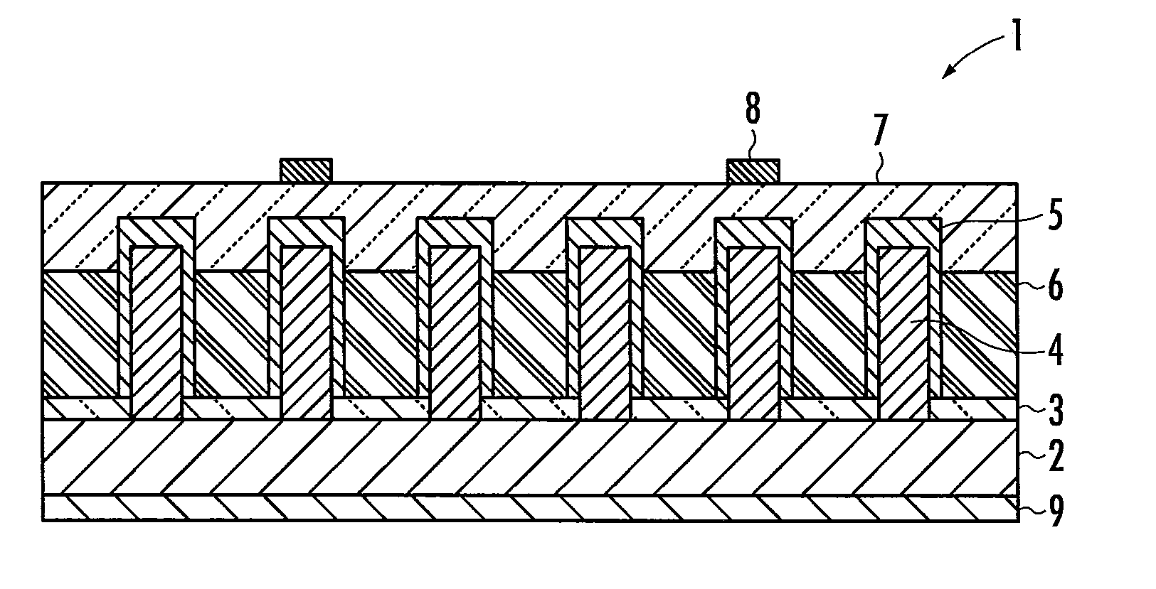
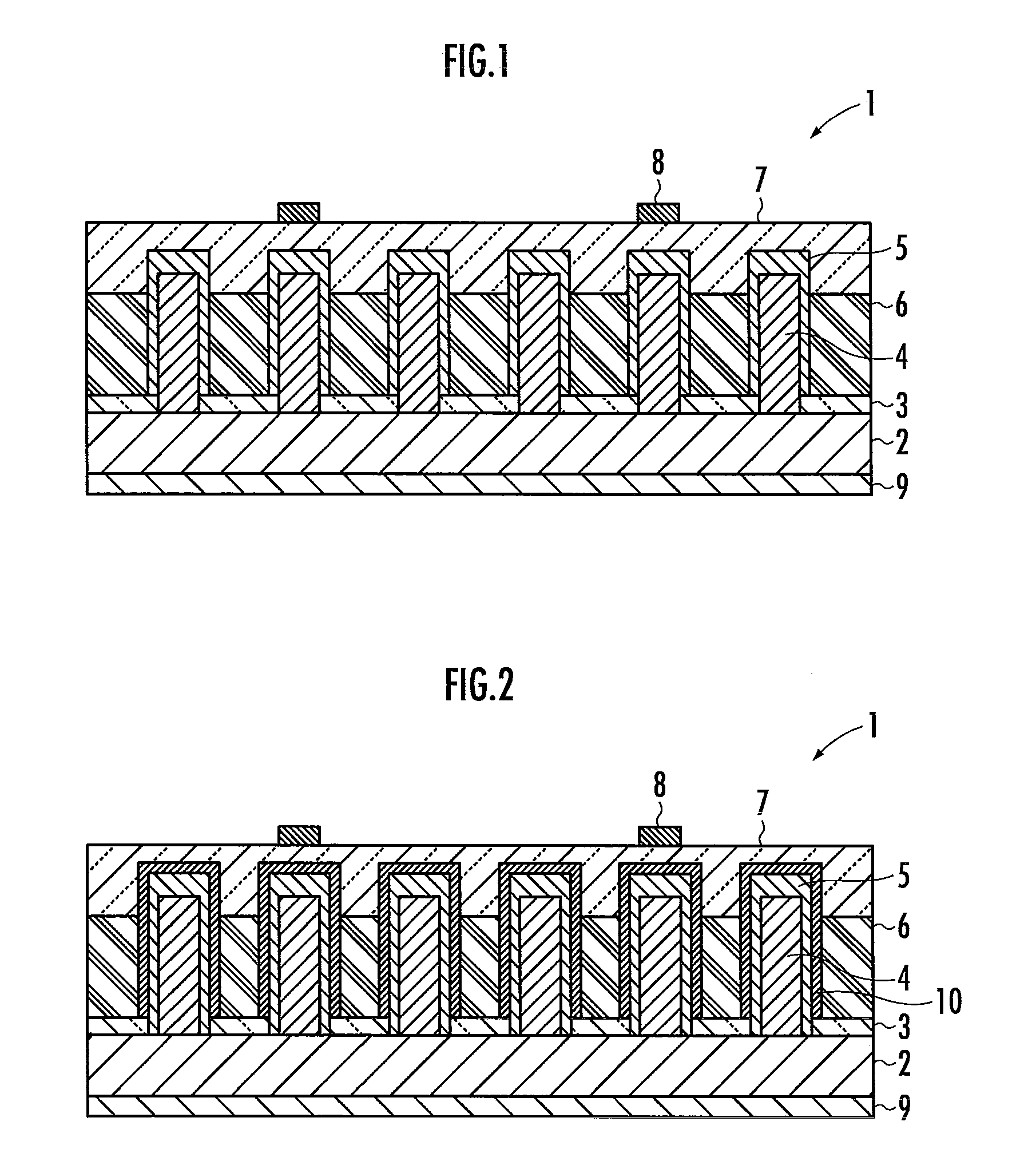
[0030]First, a nanowire photovoltaic cell 1 according to the present invention will be described with reference to FIG. 1. The nanowire photovoltaic cell 1 is provided with an InP (111) A substrate 2, an amorphous SiO2 film 3 formed on the InP (111) A substrate 2, and a p-type InP nanowire semiconductor 4 formed on a portion of the InP (111) A substrate 2 uncoated by the amorphous SiO2 film 3. The p-type InP nanowire semiconductor 4 has an n-type InP semiconductor 5 formed along the surface thereof. Between the p-type InP semiconductor 4 and the n-type InP semiconductor 5, there is provided an i-type InP semiconductor (not shown). Thereby, the nanowire photovoltaic cell 1 has a core-shell structure with the p-type InP semiconductor 4 served as a core, the i-type InP semiconductor and the n-type InP semiconductor served as a shell.

[0031]The nanowire photovoltaic cell 1 is further provided with a transparent insulator 6 filled between gaps of a plurality of the p-type InP nanowire sem...

second embodiment

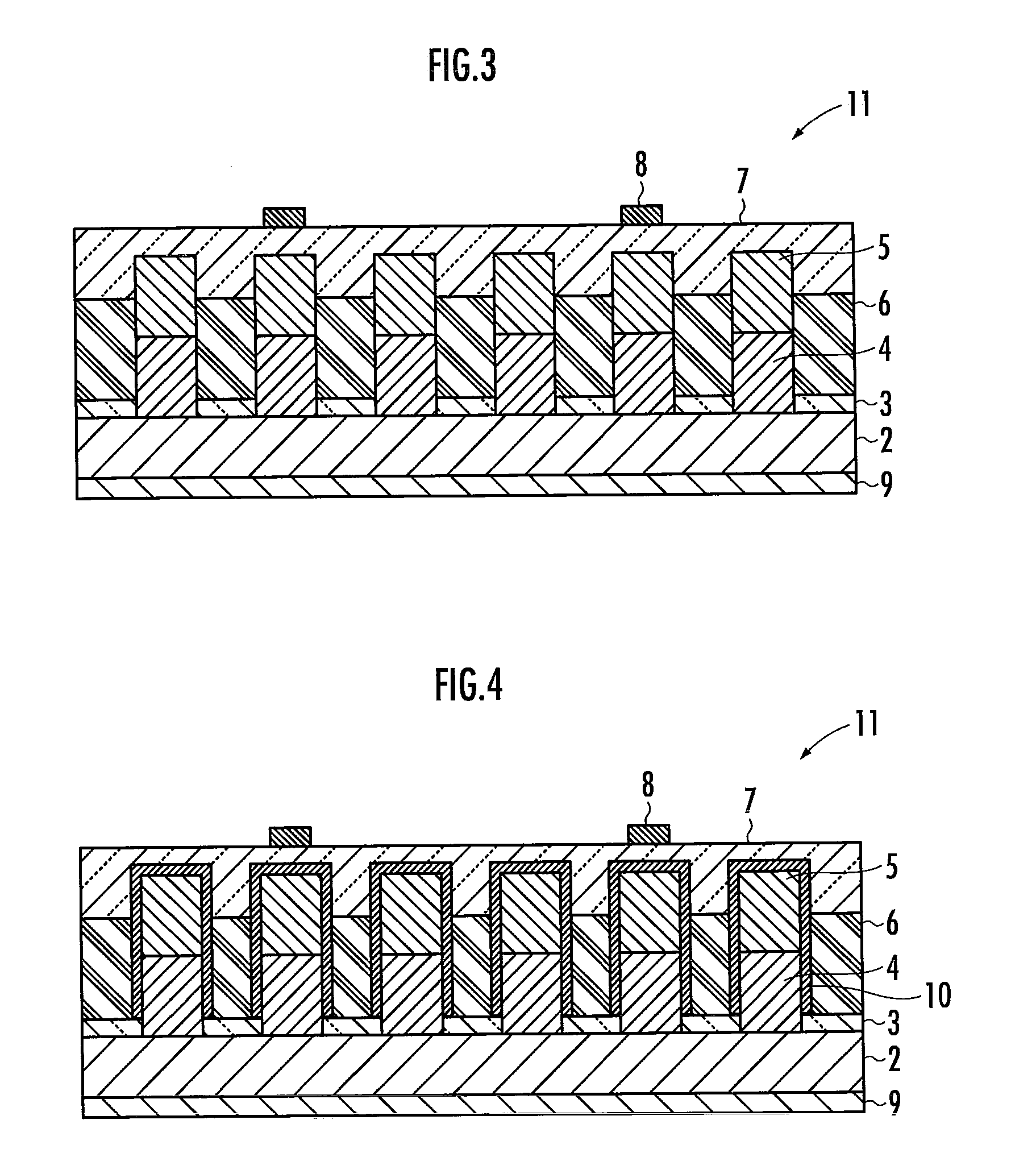
[0034]Hereinafter, a nanowire photovoltaic cell 11 according to the present invention will be described with reference to FIG. 3. The nanowire photovoltaic cell 11 has the same structure as the nanowire photovoltaic cell 1 in FIG. 1, except that the n-type InP semiconductor 5 is joined with the p-type InP nanowire semiconductor 4 in the lengthwise direction to form the PN junction. In addition, between the p-type InP semiconductor 4 and the n-type InP semiconductor 5, there is provided an i-type InP semiconductor (not shown).

[0035]As illustrated in FIG. 4, it is also acceptable for the nanowire photovoltaic cell 11 to have the passivation layer 10 disposed on the either surface of the p-type InP nanowire semiconductor 4, the i-type InP semiconductor and the n-type InP semiconductor 5. As illustrated in FIG. 4, it is acceptable to cover totally the p-type InP semiconductor 4, the i-type InP semiconductor and the n-type InP semiconductor 5 above the amorphous SiO2 film 3 with the pass...


PUM

PropertyMeasurementUnit
Vocaaaaaaaaaa
thicknessaaaaaaaaaa
diameteraaaaaaaaaa

Abstract

Provided is a nanowire photovoltaic cell (1) including a semiconductor substrate (2) and a plurality of nanowire semiconductors (4) and (5) having a PN junction. The semiconductor substrate (2) and the nanowire semiconductors (4) and (5) are composed of one single crystal. The manufacture method of the nanowire photovoltaic cell includes a step of coating a part of a surface of the semiconductor substrate (2) with an amorphous film (3), and a step of developing a crystal of a material identical to that of the semiconductor substrate (2) through epitaxial growth on the uncoated surface of the semiconductor substrate (2) to form the plurality of nanowire semiconductors (4) and (5).

Description

BACKGROUND OF THE INVENTION[0001]1. Field of the Invention[0002]The present application relates to a nanowire photovoltaic cell composed of a nanowire semiconductor and a manufacture method thereof.[0003]2. Description of the Related Art[0004]It is known that a photovoltaic cell in general has a planar PN junction interface parallel to a surface of a substrate. Compared to the general photovoltaic cell, there has been known in recent years a photovoltaic cell composed of a fine linear semiconductor having a diameter of a nanometer order, commonly called as a nanowire, a nanorod and the like (hereinafter, described as nanowire photovoltaic cell).[0005]There has been proposed a technique to make uneven the PN junction interface to improve the photoelectric conversion efficiency of the nanowire photovoltaic cell. According to the nanowire photovoltaic cell with the PN junction interface made uneven, since the area of the PN junction interface is made greater than that of a light accept...

Claims


Application Information

Patent Timeline
Patent Type & Authority Applications(United States)
IPC IPC(8): H01L31/00H01L31/18
CPCH01L31/03529Y02E10/547H01L31/1804Y02P70/50
Inventor GOTO, HAJIMEOHASHI, TOMOAKIMOTOHISA, JUNICHIFUKUI, TAKASHI
Owner HONDA MOTOR CO LTD
Why Eureka
Try Eureka