Metal oxide semiconductor devices having implanted carbon diffusion retardation layers and methods for fabricating the same

a technology of carbon diffusion retardation and metal oxide semiconductors, which is applied in the direction of semiconductor devices, electrical devices, transistors, etc., can solve the problems of increasing the risk that dopants may diffuse into the channel during subsequent processing, increasing the risk of dopant species diffraction relatively long distances from the implanted region, and undesirable short channel effects

Inactive Publication Date: 2010-01-21
GLOBALFOUNDRIES INC
View PDF3 Cites 150 Cited by
  • Summary
  • Abstract
  • Description
  • Claims
  • Application Information

AI Technical Summary

Problems solved by technology

However, reducing the thickness of spacers decreases the separation between the channel and doped source/drain regions, thereby increasing the risk that dopants may diffuse into the channel during subsequent processing.
In particular, post-implant annealing processes that subject devices to a considerable thermal budget of time and temperature may cause dopant species to diffuse relatively long distances from implanted regions.
Advanced devices having narrowed spacers characteristic of the 45 nm technology node and beyond are especially susceptible to this condition as even low concentrations of either P-type S/D dopants (for PMOS device

Method used


Image

  • Metal oxide semiconductor devices having implanted carbon diffusion retardation layers and methods for fabricating the same
  • Metal oxide semiconductor devices having implanted carbon diffusion retardation layers and methods for fabricating the same
  • Metal oxide semiconductor devices having implanted carbon diffusion retardation layers and methods for fabricating the same

Examples


Embodiment Construction

[0010]The following detailed description of the invention is merely exemplary in nature and is not intended to limit the invention or the application and uses of the invention. Furthermore, there is no intention to be bound by any theory presented in the preceding background of the invention or the following detailed description of the invention.

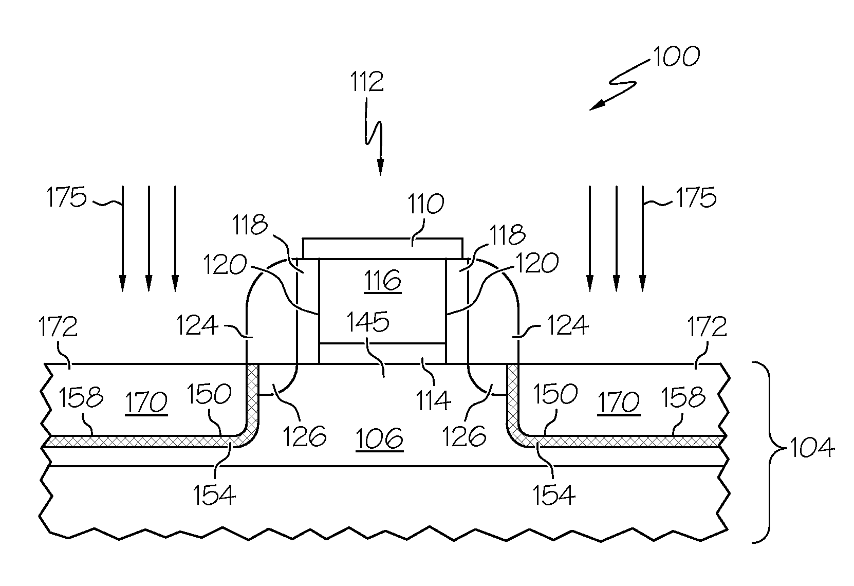
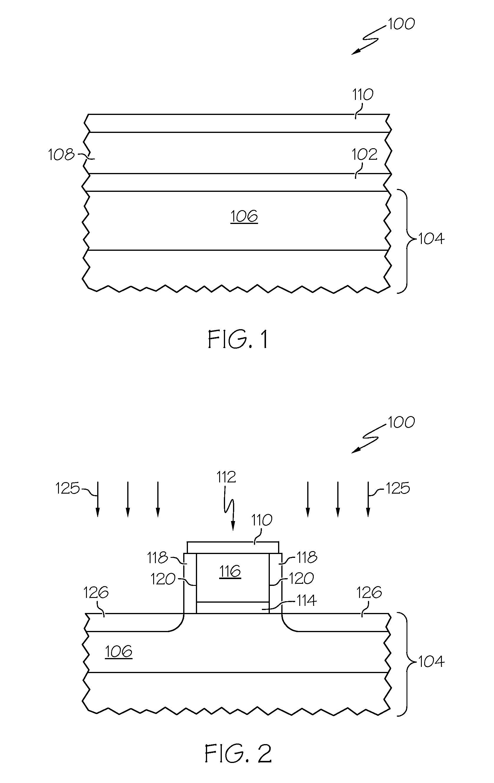
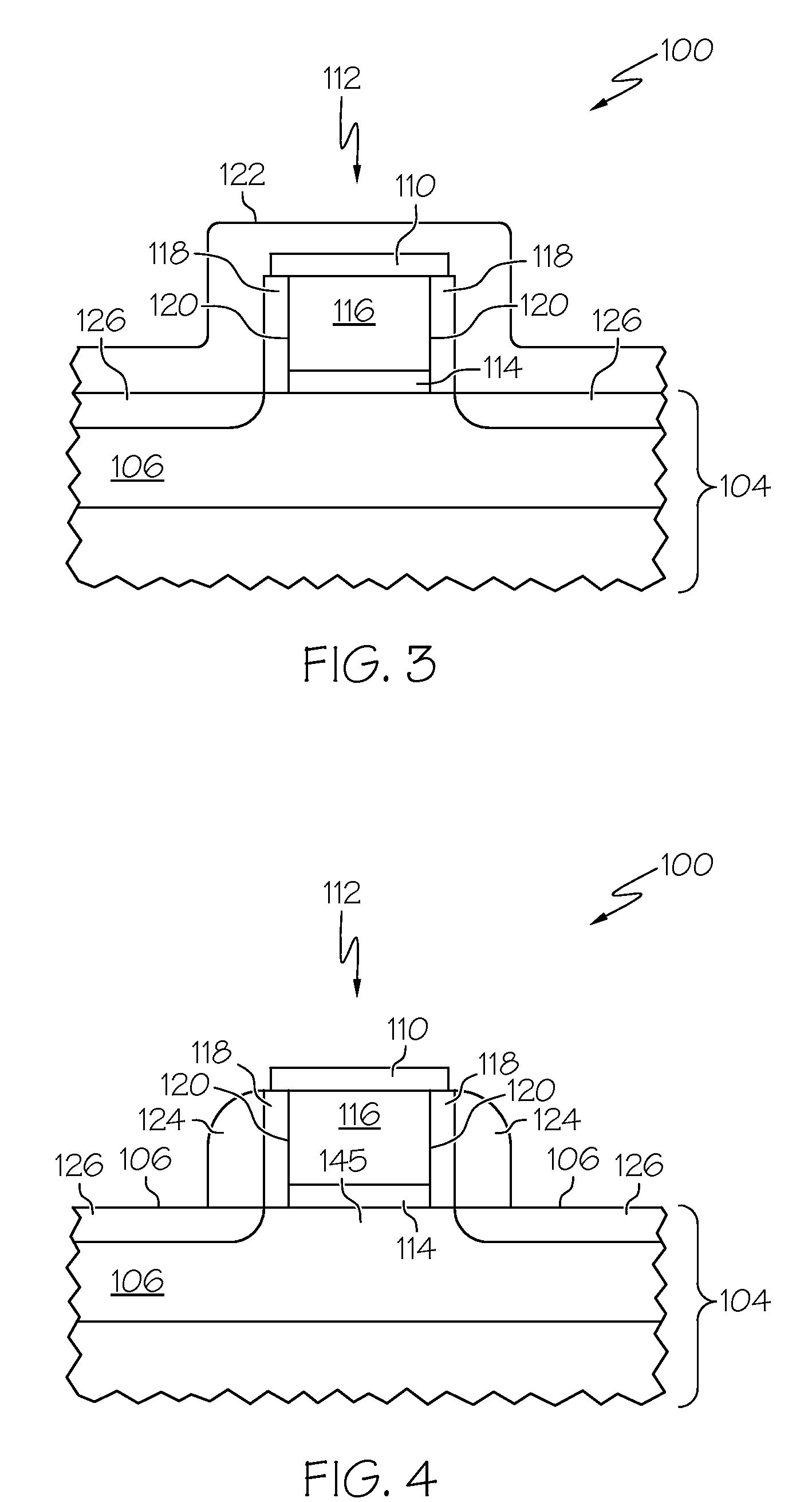
[0011]The various embodiments of the present invention result in the fabrication of an MOS transistor having a carbon-comprising, diffusion-retardation layer disposed underlying the deep source and drain regions to reduce the diffusion rate of source / drain impurity dopants such as phosphorous, arsenic, or boron. The diffusion retardation layer significantly reduces the diffusion coefficient of dopants within the layer and thereby reduces the range of dopant diffusion during high temperature annealing processes and, accordingly, the risk of dopant diffusion into the channel region of a MOS device. Further, because the rate of diffusion of dop...


PUM


Abstract

Semiconductor devices and methods for fabricating semiconductor devices are provided. One exemplary method comprises providing a silicon-comprising substrate having a first surface, etching a recess into the first surface, the recess having a side surface and a bottom surface, implanting carbon ions into the side surface and the bottom surface, and forming an impurity-doped, silicon-comprising region overlying the side surface and the bottom surface.

Description

FIELD OF THE INVENTION[0001]The present invention generally relates to semiconductor devices and methods for fabricating semiconductor devices, and more particularly relates to metal oxide semiconductor devices having implanted carbon diffusion-retardation layers and methods for fabricating such semiconductor devices.BACKGROUND OF THE INVENTION[0002]As the pitch between individual devices on integrated circuits (ICs) continues to shrink with each new technology generation, components of these devices including gate electrodes and spacers are scaled down in size accordingly. Spacers used as masks for source and drain implantation processes provide a self-alignment of the source and drain (S / D) to the gate electrode and shadow the channel region from impinging dopant ions. Spacers thereby play a critical role in creating desirable dopant profiles in the source and drain and keep the S / D dopant from the channel to prevent S / D punch through. However, reducing the thickness of spacers de...

Claims


Application Information

Patent Timeline
IPC IPC(8): H01L29/00H01L21/8236
CPCH01L21/26506H01L21/26513H01L21/26586H01L29/165H01L29/7848H01L29/66628H01L29/66636H01L29/7833H01L29/6659
Inventor YANG, FRANK BINHARGROVE, MICHAEL J.PAL, ROHIT
Owner GLOBALFOUNDRIES INC
Why Eureka
Try Eureka