Method and Apparatus for Inspecting Defects

a defect detection and defect technology, applied in the direction of optical radiation measurement, instruments, measurement devices, etc., can solve the problems of defect detection performance decline, and difficulty in high sensitivity detection of short-circuit defects at the bottom of patterns, and achieve high-precision defect detection

Inactive Publication Date: 2010-01-21
HITACHI HIGH-TECH CORP
View PDF10 Cites 20 Cited by
  • Summary
  • Abstract
  • Description
  • Claims
  • Application Information

AI Technical Summary

Benefits of technology

[0008]The present invention for solving the above problems provides a defect inspection method and defect inspection apparatus capable of achieving highly accurate defect detection by controlling polarization of illumination light according to scattered-light characteristics of defects to be detected.

Problems solved by technology

There have been the problems, however, that if the wafer includes patterns and the pattern pitch is shorter than the wavelength of the light, since the semiconductor patterns themselves will have polarizing characteristics, the polarization characteristics of the light diffracted from the patterns will also change and defect detection performance will decrease as a result.
For a wafer with vertically long patterns, in particular, short-circuiting defects at the bottoms of the patterns have been difficult to detect with high sensitivity.

Method used


Image

  • Method and Apparatus for Inspecting Defects
  • Method and Apparatus for Inspecting Defects
  • Method and Apparatus for Inspecting Defects

Examples


second embodiment

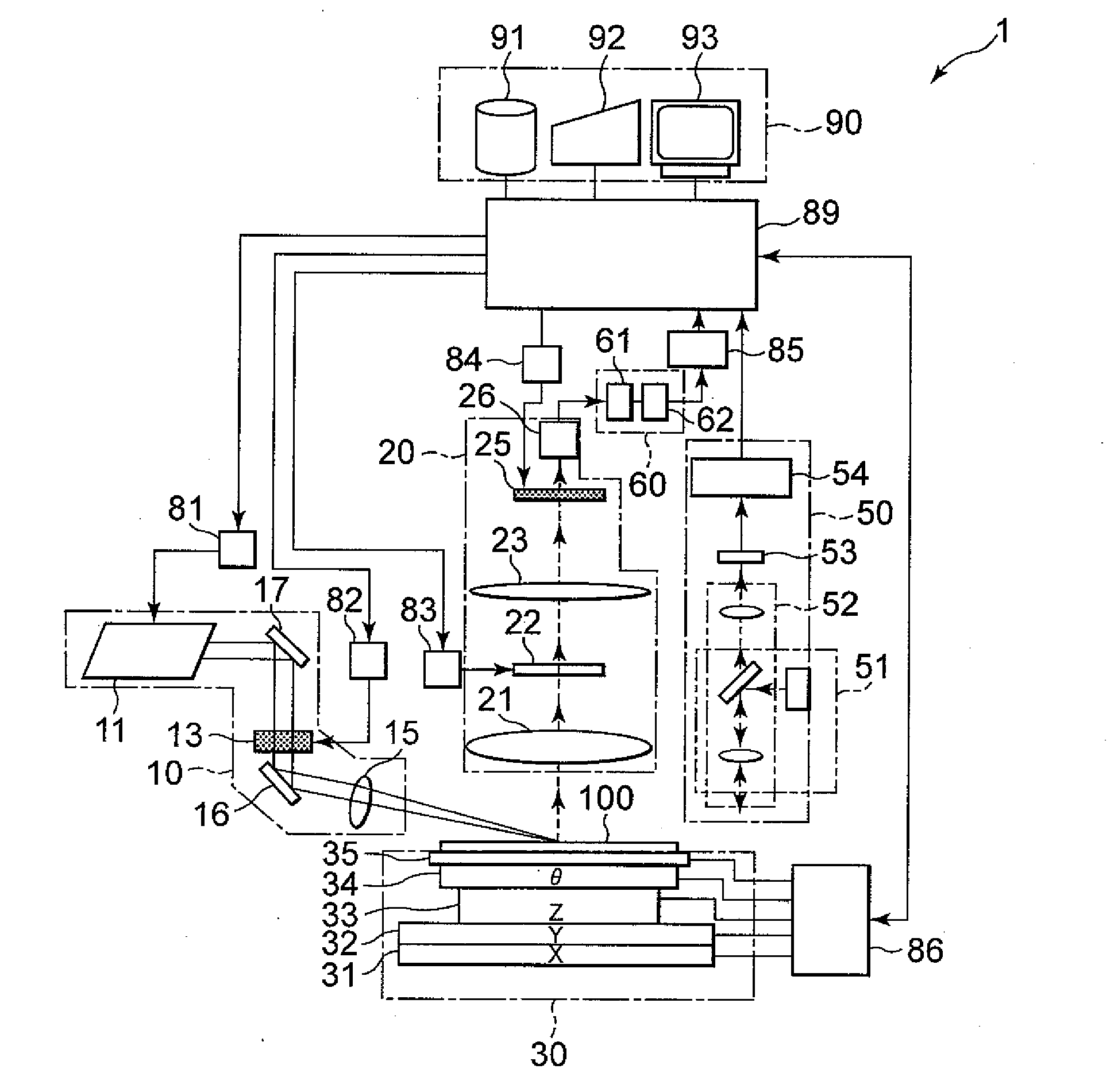
[0099]A second embodiment of an inspection apparatus according to the present invention is described below with reference to FIG. 15, a block diagram of the inspection apparatus. In the description below, the same constituent elements as those of the first embodiment are omitted and focus is placed primarily upon differences. The inspection apparatus 1 includes, as appropriate, first illumination optics 10, second illumination optics 1510, detection optics 20, a substrate conveying circuit 30, a focal measuring circuit 50 (not shown), an image-processing circuit 60, a control and processing circuit, and an interface circuit 90.

[0100]The first illumination optics 10 is constructed using, as appropriate, a laser light source 11, reflecting mirrors 16 and 17 that guide in a required direction the light emitted from the laser light source 11, a polarization control unit 13, a condensing lens 15, and an optical splitting element 1501 provided between the reflecting mirror 17 and the pola...


PUM


Abstract

An apparatus for inspecting a substrate surface is provided, which includes illumination optics for irradiating the substrate surface linearly with rectilinearly polarized light from an oblique direction, detection optics for acquiring images of the substrate surface, each of the images being formed by the light scattered from the light-irradiated substrate surface, and means for comparing an image selected as an inspection image from the plurality of substrate surface images that the detection optics has acquired to detect defects, and another image selected from the plural images of the substrate surface as a reference image different from the inspection image; the illumination optics being formed with polarization control means for controlling a polarizing direction of the light according to a particular scanning direction of the substrate or a direction orthogonal to the scanning direction.

Description

BACKGROUND OF THE INVENTION [0001]The present invention relates generally to defect inspection methods and apparatus for detecting microstructured pattern defects, contamination, and the like, by comparing an optically acquired image of an object to be inspected, and a reference image. More particularly, the invention relates to a method and apparatus for inspecting defects in a semiconductor device, a photomask, a liquid crystal, and other objects, in optical technique.[0002]During the manufacture of a semiconductor device, a substrate (wafer) on which the semiconductor device is to be formed undergoes processing through hundreds of manufacturing process steps to become a product. In these process steps, for example, if any kinds of contamination sticking to the surface of the substrate (wafer) are found or if the nonuniformity of pattern formation between processes occurs, these undesirable events will cause pattern defects, rendering the semiconductor device defective. In additio...

Claims


Application Information

Patent Timeline
Patent Type & Authority Applications(United States)
IPC IPC(8): G01J4/00
CPCG01N21/9501G01N2021/8848G01N2021/4792
Inventor UENO, TAKEONAKANO, HIROYUKIYOSHITAKE, YASUHIRO
Owner HITACHI HIGH-TECH CORP
Why Eureka
Try Eureka