Electrophotographic Photosensitive Member and Image Forming Apparatus Provided with the Same
- Summary
- Abstract
- Description
- Claims
- Application Information
AI Technical Summary
Benefits of technology
Problems solved by technology
Method used
Image
Examples
example 1
[0129]In the present example, the electrophotographic photosensitive member was manufactured as described below, and evaluation was performed with respect to surface roughness and composition of the surface layer, and dynamic indentation hardness at the boundary surface between the surface layer and the photoconductive layer. Evaluation was also performed with respect to wear volume and image deletion at the electrophotographic photosensitive member.
[0130][Manufacture of Electrophotographic Photosensitive Member]
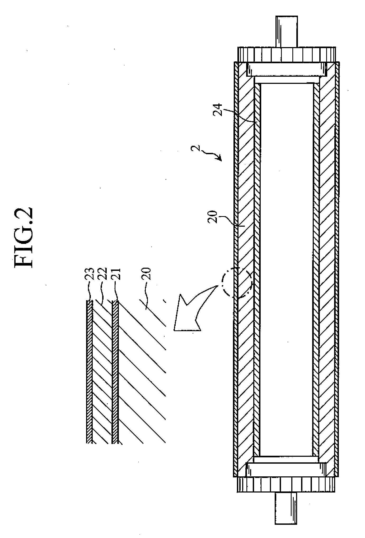
[0131]An electrophotographic photosensitive member for the present example was made by forming an anti-charge injection layer, a photoconductive layer, and a surface layer on the surface of a cylindrical body.
[0132]The cylindrical body was prepared by making a drawn tube of aluminum alloy with outer diameter of 30 mm, length of 340 mm and thickness of 1.5 mm, and then performing mirror finishing on the circumferential outer surface of the drawn tube before cleaning.
[0133]The...
example 2
[0147]In the present example, photosensitive members A′, D′, E′, F′ were made without forming the surface layers, under the same conditions as those of the photosensitive members A, D, E, F in Example 1, and surface roughness of the photoconductive layers was measured by AFM. Measurement results of the surface roughness of the photoconductive layers are shown in the following Table 6, together with the measurement results of the surface roughness of the surface layers in Example 1.
TABLE 6Surface Roughness Measured by AFMSampleRa(nm)Rz(nm)A5.5128.4A′5.3526.8D9.5145.2D′8.9242.5E14.6373.0E′15.0669.5F16.6382.6F′16.2176.3
[0148]As can be seen from Table 6, the surface roughness of the photoconductive layers of the photosensitive members A′, D′, E′, F′ without surface layers is substantially the same as the surface roughness of the surface layers of the photosensitive members A, D, E, F. Thus, it can be said that each of the photosensitive members has the same roughness at the photoconduct...
example 3
[0149]In present example, AFM photographs of the surfaces of a cylindrical body which is the same as the cylindrical bodies of the photosensitive members, and the surfaces of the photosensitive members A, D, E, F were taken. The AFM photographs were taken using “NanoScope” manufactured by Digital instrument. FIG. 3 shows the AFM photograph of the cylindrical body, and FIGS. 4 through 7 show the AFM photographs of the photosensitive members A, D, E, F, respectively. The photographs shown in FIGS. 3 through 7 are images in 10 μm square.
[0150]As can be seen from FIGS. 4 and 5, in the photosensitive members A, D, fine projections formed on the surfaces of the photosensitive members (surface layers) are smaller than those in the photosensitive members E, F. This may be considered due to ion sputtering effect in film forming. In the photosensitive members A, D, since the fine projections on the surface are relatively small, discharge products are unlikely to attach thereon, and discharge ...
PUM
 Abstract
Description
Claims
Application Information


