Pll circuit, communication device, and loopback test method of communication device

a communication device and circuit technology, applied in the direction of line-transmission details, synchronisation signal speed/phase control, transmission monitoring, etc., to achieve the effect of suppressing the jitter of the ss

Inactive Publication Date: 2010-02-04
RENESAS ELECTRONICS CORP
View PDF13 Cites 14 Cited by
  • Summary
  • Abstract
  • Description
  • Claims
  • Application Information

AI Technical Summary

Benefits of technology

[0018]In the PLL circuit according to the first exemplary aspect of the present invention, in generating the feedback clock signal by dividing the frequency of the output clock signal, a phase step width generated in the feedback clock (difference between a total phase shift amount in one period of the feedback clock and a total phase shift amount in a previous one period) can be suppressed to be equal to or less than one basic delay amount. Thus, a smooth transition of the modulation degree of the SSC is made possible while suppressing the jitter of the SSC.

Problems solved by technology

However, the patent document 2 dose not disclose the configuration in which a phase-shifted clock signal is fed back to a phase comparator through a frequency divider, and there is no suggestion to solve the above-described problem.

Method used


Image

  • Pll circuit, communication device, and loopback test method of communication device
  • Pll circuit, communication device, and loopback test method of communication device
  • Pll circuit, communication device, and loopback test method of communication device

Examples


first exemplary embodiment

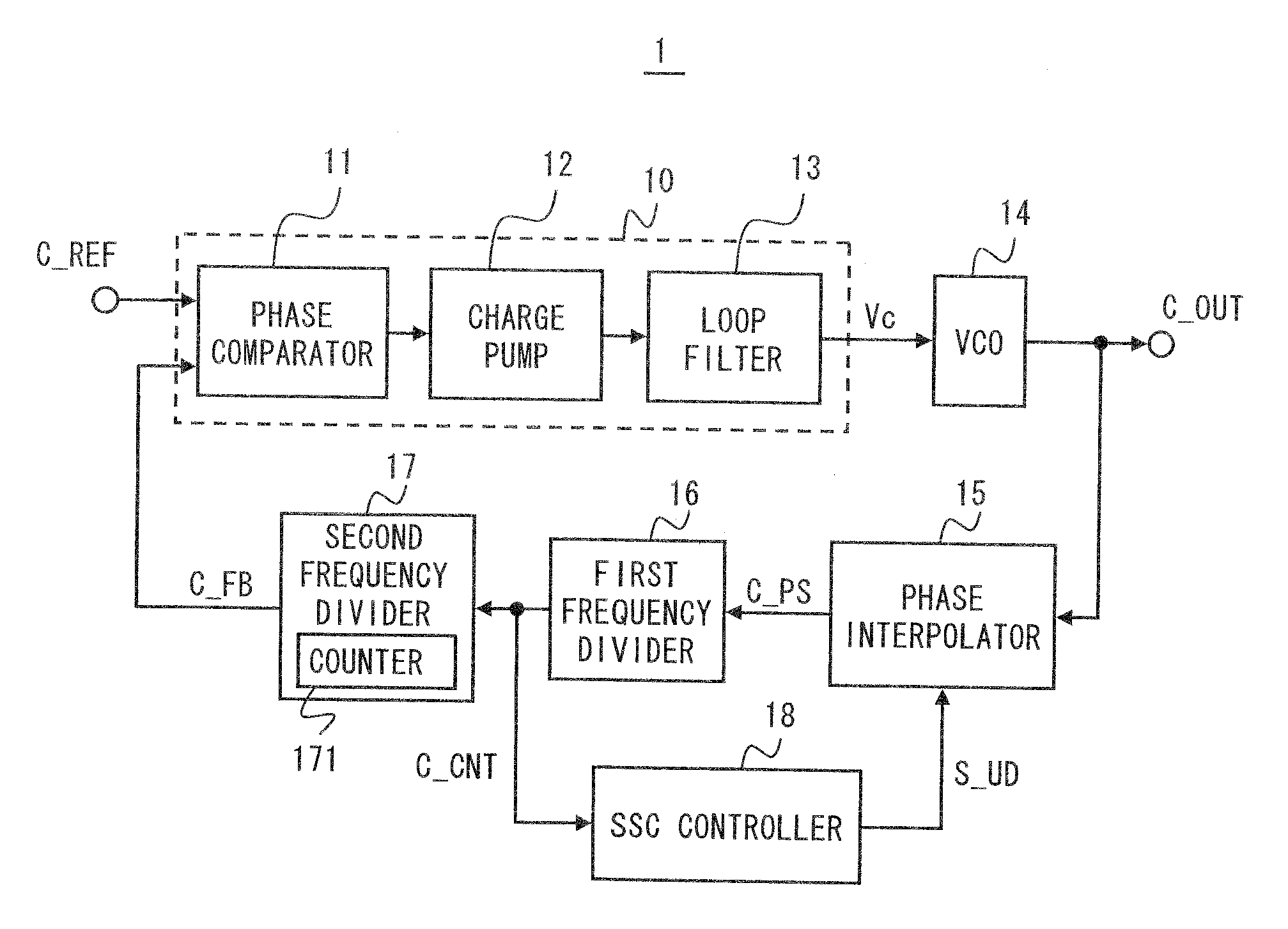
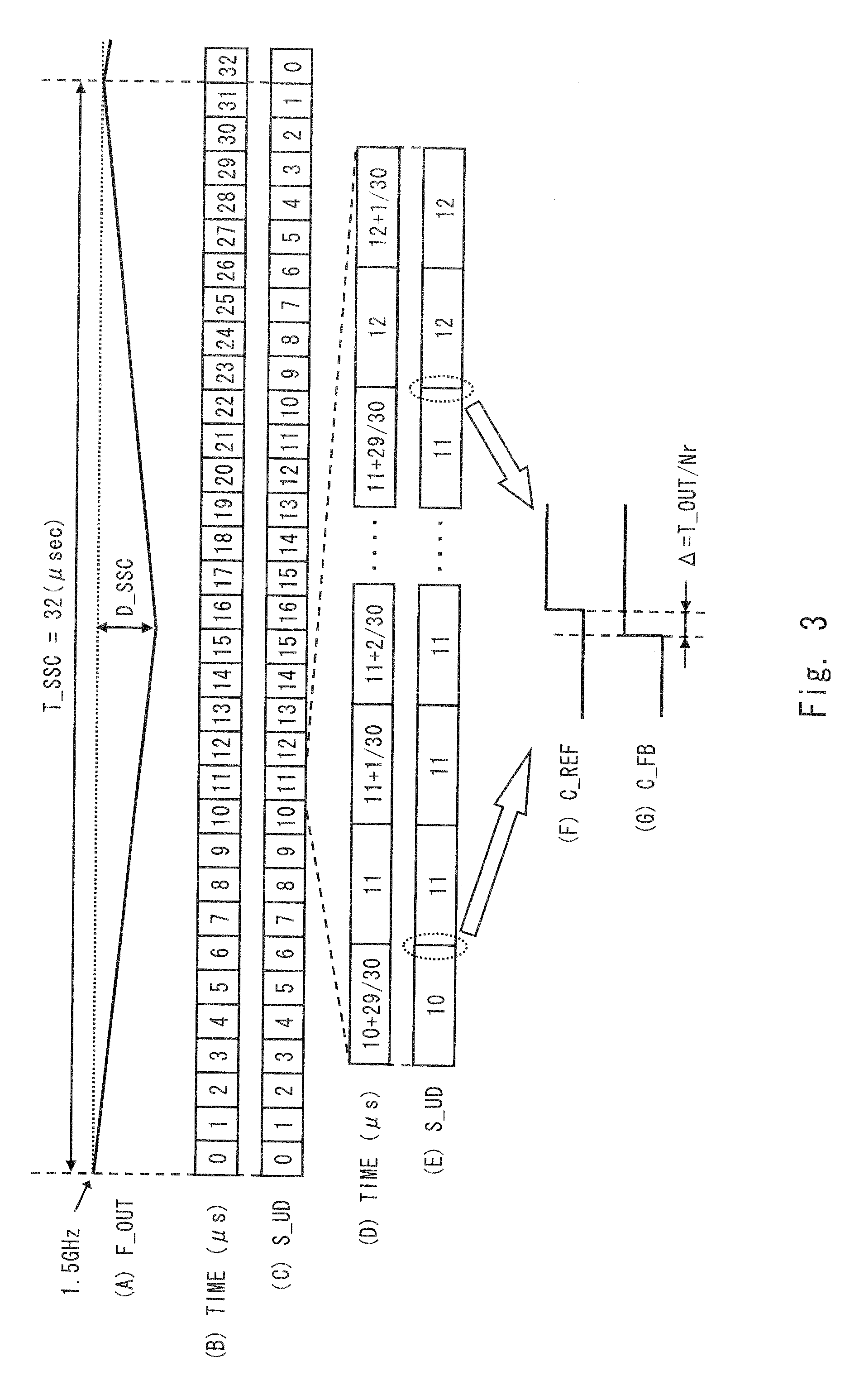
[0031]FIG. 1 is a block diagram showing the configuration of a PLL circuit 1 according to the first exemplary embodiment. The operation of the PLL circuit 1 to generate a spread spectrum output clock signal C_OUT will now be described. The PLL circuit 1 periodically increases or decreases a phase difference between a reference clock signal C_REF and a feedback clock signal C_FB input to a phase comparing unit 10 by advancing or retarding phase of the output clock signal C_OUT of a VCO 14 by a phase interpolator 15 that is arranged on a feedback path. In accordance with this periodical fluctuation of the phase difference, a control voltage Vc supplied from the phase comparing unit 10 to the VCO 14 periodically increases or decreases, and the output clock signal C_OUT is frequency-modulated. In the following description, each component shown in FIG. 1 will be described.

[0032]The phase comparing unit 10 receives C_REF and C_FB, and generates a control voltage Vc in accordance with the ...

second exemplary embodiment

[0070]In the second exemplary embodiment, description will be made of the improvement of the phase shift control by the SSC controller 18 described above. Note that the configuration of the PLL circuit according to the second exemplary embodiment may be similar to that of the PLL circuit 1 shown in FIG. 1. Accordingly, description and explanation of the whole block diagram of the PLL circuit according to the second exemplary embodiment will be omitted In the following description, a configuration example and the operation of an SSC controller 28 included in the PLL circuit according to the second exemplary embodiment will be described.

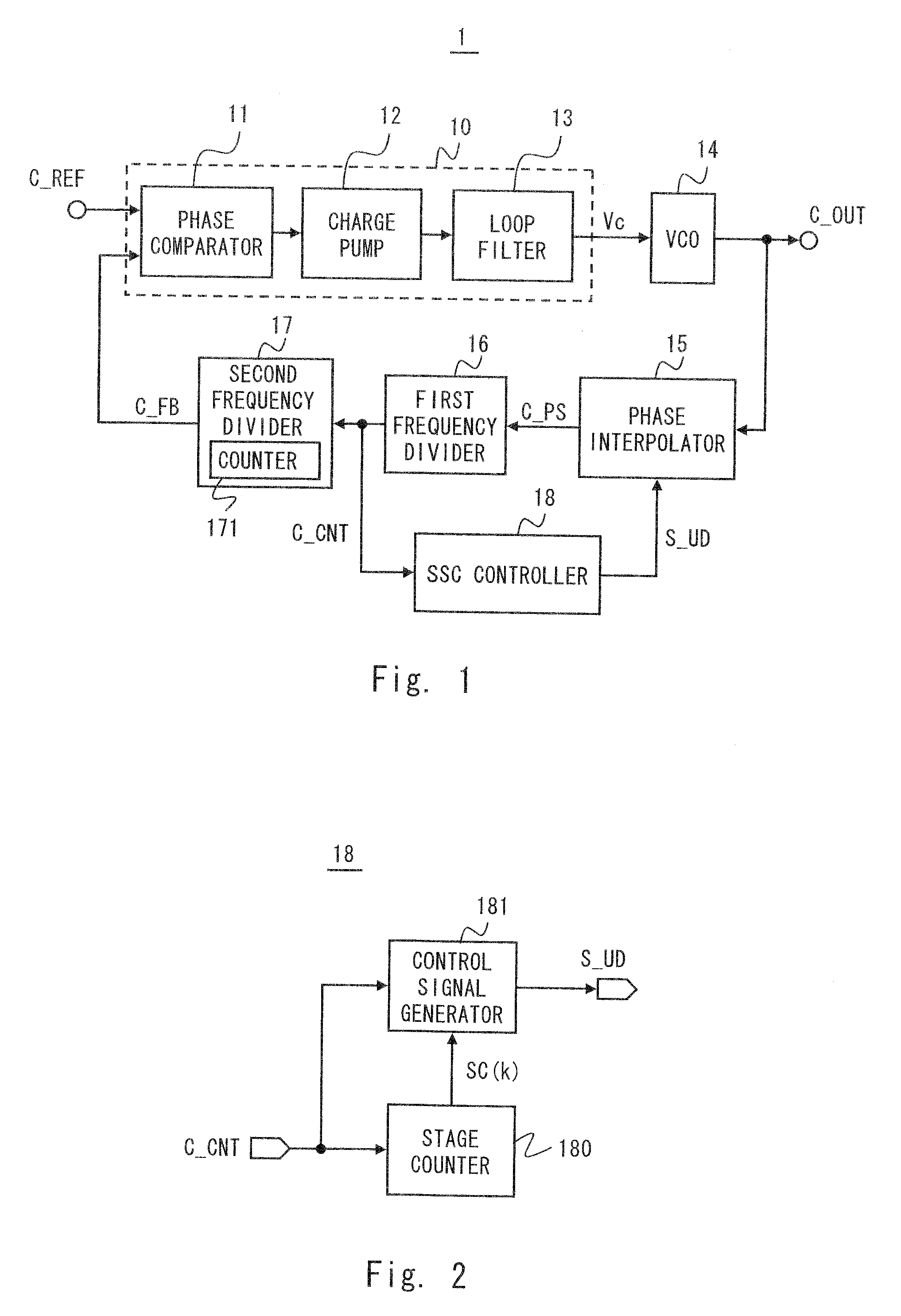
[0071]FIG. 5 is a block diagram showing a configuration example of the SSC controller 28. The stage counter 180 and the control signal generator 181 shown in FIG. 5 are similar to those shown in FIG. 2. A fractional counter 280 is arranged between the stage counter 180 and the control signal generator 181. The fractional counter 280 generates the fract...

third exemplary embodiment

[0075]FIG. 7 shows the configuration of a communication device 30 according to the third exemplary embodiment. In FIG. 7, a PLL circuit 3 has the configuration similar to that of the PLL circuit 1 of the first exemplary embodiment described above. However, as shown in FIG. 8, the PLL circuit 3 includes a line and a terminal to supply the phase shift signal C_PS generated by the phase interpolator 15 to a transmitting unit 301.

[0076]The transmitting unit 301 transmits a data signal such as SATA (Serial ATA) or the like, for example. The transmitting unit 301 is arranged so as to be able to receive C_OUT and C_PS supplied from the PLL circuit 3, and is operated by any one of the two clock signals selectively supplied. The switching of the operational clock signal supplied to the transmitting unit 301 may be made possible, for example, by a switch, a jumper pin or the like operable from outside the communication device 30. Further, switching of the operational clock signal supplied to ...


PUM


Abstract

A controlling unit disposed in a PLL circuit controls a phase interpolator to gradually change a phase shift amount applied to a phase shift signal C_PS by a unit of basic delay amount Δ at a timing predetermined in accordance with a modulation profile of an SSC. Further, the controlling unit controls a total phase shift amount applied to the phase shift signal C_PS output from the phase interpolator in one period of a feedback clock signal C_FB obtained by dividing frequency of the phase shift signal C_PS in a way that a difference between the total phase shift amount and a total phase shift amount in a previous one period of C_FB is always equal to or less than the basic delay amount Δ.

Description

BACKGROUND OF THE INVENTION[0001]1. Field of the Invention[0002]The present invention relates to a PLL (Phase Locked Loop) circuit that generates a spread spectrum clock, and a communication device using the same.[0003]2. Description of Related Art[0004]A spread spectrum clock (SSC) signal has been generally employed in order to suppress occurrence of EMI (Electro Magnetic Interference) by electronic devices. For example, an SSC is generated by modulating frequency of a clock signal generated by a PLL circuit or the like in accordance with a predetermined modulation frequency and modulation degree. Patent documents 1 to 5 listed below disclose a device that generates an SSC.[0005]Patent document 1: Japanese Unexamined Patent Application Publication No. 2006-166049[0006]Patent document 2: U.S. Pat. No. 6888412[0007]Patent document 3: Japanese Patent No. 4074166[0008]Patent document 4: Japanese Unexamined Patent Application Publication No. 2007-6121[0009]Patent document 5: Japanese Un...

Claims


Application Information

Patent Timeline
Patent Type & Authority Applications(United States)
IPC IPC(8): H04B1/69H03D3/24H04B3/46H03C3/00H03L7/08H03L7/18
CPCH03L7/0891H03L7/197H03L7/18H03L7/0998H04L7/06
Inventor OGASAWARA, KAZUONAKADAIRA, MASAO
Owner RENESAS ELECTRONICS CORP
Why Eureka
Try Eureka