Systematic, normalized metric for analyzing and comparing optimization techniques for integrated circuits employing voltage scaling and integrated circuits designed thereby

a voltage scaling and optimization technique, applied in the field of systemic, normalized metric for analyzing and comparing optimization techniques of integrated circuits, can solve the problems of reducing the speed at which signals propagate through the circuit, circuits may not operate as fast as needed or desired, and ic fabrication costs generally decreas

Inactive Publication Date: 2010-02-11
BELL SEMICON LLC
View PDF10 Cites 21 Cited by
  • Summary
  • Abstract
  • Description
  • Claims
  • Application Information

AI Technical Summary

Problems solved by technology

Unfortunately, using lower leakage current cells or lower drive voltages almost always reduces the speed at which signals propagate through the circuit.
Consequently, the circuit may not operate as fast as needed or desired.
IC fabrication cost generally decreases as IC substrate (“die”) size decreases.
Signals that propagate too slowly through the circuit cause setup violations; signals that propagate too quickly through the circuit cause hold violations.
Setup or hold violations corrupt the flow of logic through the logic of the circuit and give rise to functional errors.
Thus a fundamental tradeoff exists among speed and power consumption.
These force the circuit designer to employ EDA tools, particularly timing signoff, to strike a delicate balance.
These variations increase the degree to which the designer must ensure that production circuits work under real-world operating conditions and therefore the complexity of timing signoff.
Further complicating the designer's task is the difficulty of measuring and therefore being able to judge tradeoffs of speed and power consumption.
Some metrics are effective for one process technology, but fail to translate to other technologies.
Other metrics may apply to multiple technologies, but are difficult to understand and defy intuition.

Method used


Image

  • Systematic, normalized metric for analyzing and comparing optimization techniques for integrated circuits employing voltage scaling and integrated circuits designed thereby
  • Systematic, normalized metric for analyzing and comparing optimization techniques for integrated circuits employing voltage scaling and integrated circuits designed thereby
  • Systematic, normalized metric for analyzing and comparing optimization techniques for integrated circuits employing voltage scaling and integrated circuits designed thereby

Examples


Embodiment Construction

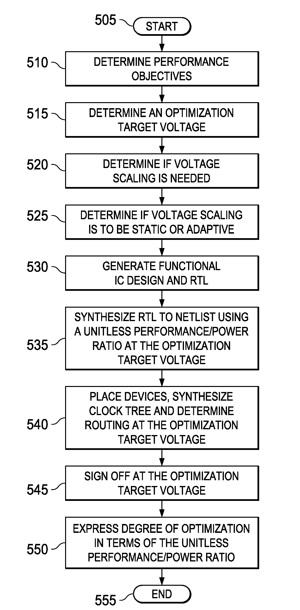
[0023]Voltage scaling, referred to in the Summary above, is a technique whereby the drive voltage to a particular IC is modulated to one or more particular values such that the IC can function properly. Voltage scaling is particularly suited to compensate for process variations. Static voltage scaling may be performed at the factory (e.g., during calibration) or before the IC begins normal operation (e.g., during powerup initialization). In contrast, adaptive voltage scaling (AVS) is performed continually while the IC is in normal operation and particularly effective at compensating for temperature variations and device aging as well as process variations. ICs can have one or more domains, each having its own voltage regulator. Drive voltage can therefore be modulated separately in each domain, allowing compensation for OCV to be carried out as well.

[0024]While voltage scaling (including AVS) is known, it has heretofore been used only to compensate for process and temperature variat...


PUM


Abstract

Various embodiments of methods of designing an integrated circuit (IC). One embodiment of one such method includes: (1) generating a functional design for the IC, (2) determining performance objectives for the IC, (3) determining an optimization target voltage for the IC, (4) determining whether the IC needs voltage scaling to achieve the performance objectives at the optimization target voltage and, if so, whether the IC is to employ static voltage scaling or adaptive voltage scaling, (5) using the optimization target voltage to synthesize a layout from the functional IC design that meets the performance objectives by employing a unitless performance / power quantifier as a metric to gauge a degree of optimization thereof and (6) performing a timing signoff of the layout at the optimization target voltage.

Description

CROSS-REFERENCE TO RELATED APPLICATION[0001]This application claims the benefit of U.S. Provisional Application Ser. No. 61 / 126,881, filed by Parker, et al., on May 7, 2008, entitled “A Novel Paradigm for Optimizing Performance, Power, Area and / or Yield in Integrated Circuits,” commonly assigned with the invention and incorporated herein by reference. This application is also related to U.S. Non-Provisional application Ser. No. [Attorney Docket No. PARKER 4-4-4-43-1, IDS #126787] filed by Parker, et al., on even date herewith, entitled “Methods for Designing Integrated Circuits Employing Voltage Scaling and Integrated Circuits Designed Thereby” and U.S. Non-Provisional application Ser. No. [Attorney Docket No. JAMANN 1-5-6, IDS #126839] filed by Jamann, et al., on even date herewith, entitled “A Systematic Benchmarking System and Method for Standardized Data Creation, Analysis and Comparison of Semiconductor Technology Node Characteristics,” commonly assigned with the invention and ...

Claims


Application Information

Patent Timeline
Patent Type & Authority Applications(United States)
IPC IPC(8): G06F17/50
CPCG01R31/31725G06F1/04G06F1/26G06F17/5081H03K19/215G06F17/505G06F1/3203G06F30/327G06F30/398
Inventor JAMANN, JOSEPH J.PARKER, JAMES C.RAO, VISHWAS M.
Owner BELL SEMICON LLC
Why Eureka
Try Eureka