Printed circuit board and method for manufacturing same

a technology of printed circuit boards and printed circuits, applied in the direction of superimposed coating process, liquid/solution decomposition chemical coating, resistive material coating, etc., can solve problems such as registration errors and easy warping

Inactive Publication Date: 2010-02-18
ZHEN DING TECH CO LTD +1
View PDF2 Cites 2 Cited by
  • Summary
  • Abstract
  • Description
  • Claims
  • Application Information

AI Technical Summary

Problems solved by technology

However, warping easily occurs in thin PCBs due to internal stress present therein, particularly in peripheral portions of the PCBs, which finally may cause registration errors during a manufacturing process of the PCBs, or an assembling process of PCB with other electronic elements.

Method used


Image

  • Printed circuit board and method for manufacturing same
  • Printed circuit board and method for manufacturing same
  • Printed circuit board and method for manufacturing same

Examples


first embodiment

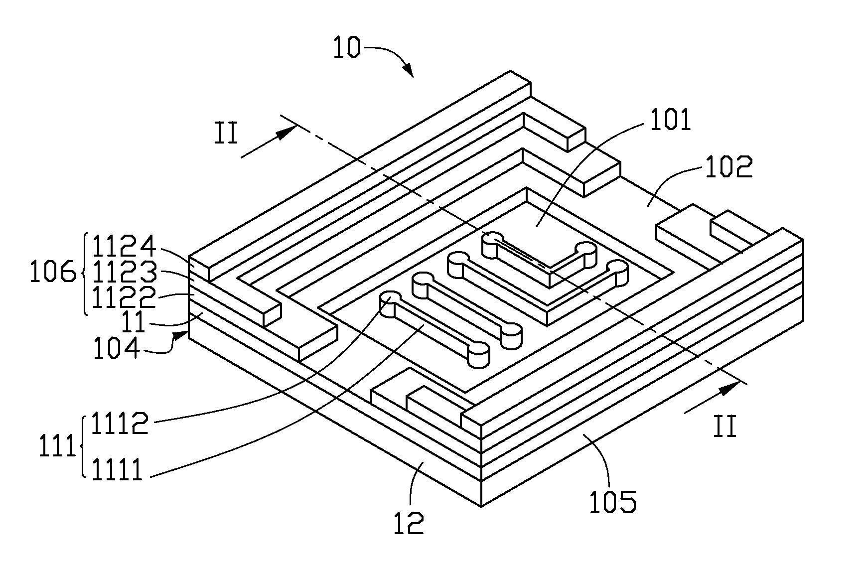
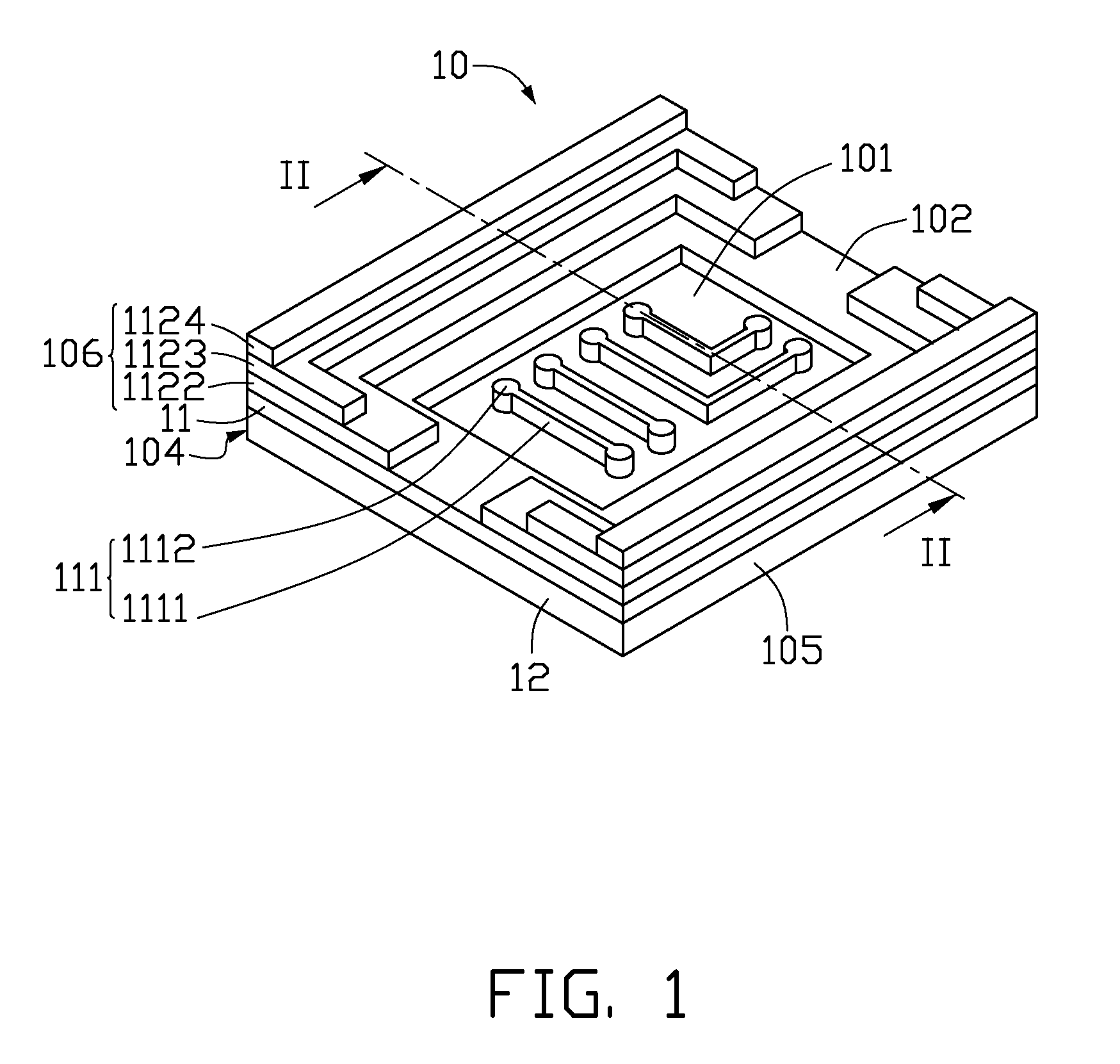
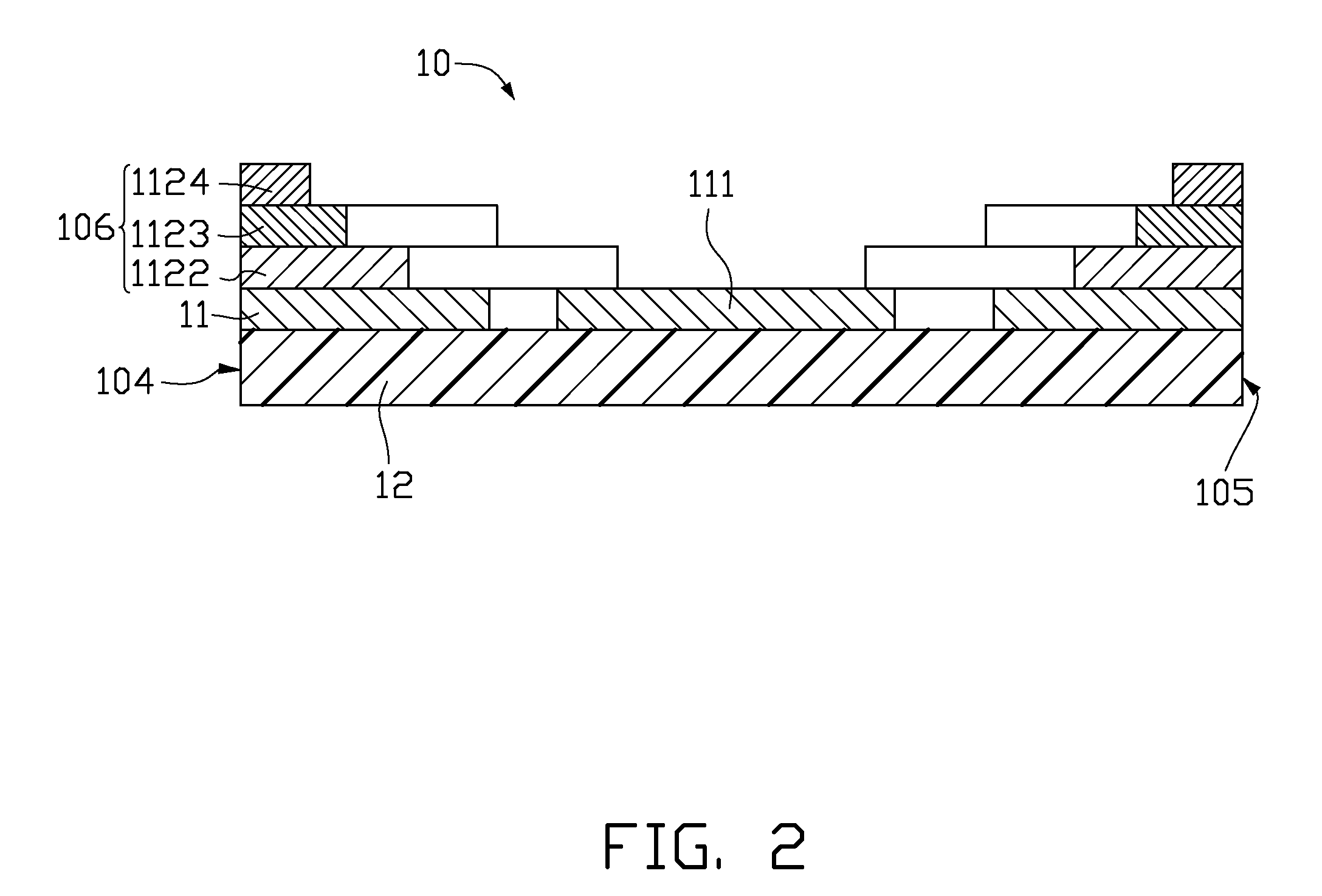
[0018]Referring to FIGS. 1 and 2, a square shaped PCB 10 provided in a first embodiment includes an insulating layer 12, a copper layer 11 and a reinforcing layer 102 disposed on the cooper layer 11. In the illustrated embodiment, the insulating layer 12 and the copper layer 11 cooperate to form a copper clad laminate (CCL). The reinforcing layer 102 is configured for counteracting and compensating internal stress present in the CCL which may otherwise cause warping deformation of the CCL. Due to the reinforcing layer 102, flatness of the CCL could readily be maintained.

[0019]The insulating layer 12 can be comprised of polyimide, polyethylene terephtalate, polytetrafluorethylene, polyaminde, polymethylmethacrylate, polycarbonate, polyamide polyethylene-terephthalate copolymer, glass fiber / resin compound, or other material. In the illustrated embodiment, the insulating layer 12 is made of polyimide, and has a first side surface 104 and an opposite second side surface 105. The PCB 10 ...

second embodiment

[0027]Referring to FIG. 10, a second PCB 20 is provided in a second embodiment, differing from the PCB 10 in that the unwanted peripheral portion 212 is single layer structured and the greatest thickness thereof is substantially equal to that of the electrical traces 211. The reinforcing layer 212 is obtained using a method comprising forming a metal layer (not shown) on the peripheral portion using an electro-less plating process or an electro-plating process and a series of known developing and etching processes after forming the electrical traces 211.

third embodiment

[0028]Referring to FIG. 11, a third PCB 30 is provided in a third embodiment, differing from the PCB 10 in that the thickness of the reinforcing layer 312 linearly increases with increasing distance to the center of the PCB 30. In this embodiment the cross-section of the reinforcing layer 312 is right-triangle shaped. The reinforcing layer 312 is obtained using a method comprising forming a metal layer (not shown) on the peripheral portion using an electro-less plating process or an electro-plating process and a surface grinding process or other method after forming the electrical traces 311. Alternatively, the reinforcing layer 312 can be some other shape in cross-section to increase or decrease the weight thereof as needed.

[0029]Furthermore, it is understood that when the PCB 30 is a rectangle shaped, the PCB 30 more easily warps in a direction parallel to a lengthwise direction thereof. Accordingly, a thickness of the reinforcing layer 312 should gradually increase in a direction...


PUM

PropertyMeasurementUnit
electricalaaaaaaaaaa
thicknessaaaaaaaaaa
insulatingaaaaaaaaaa

Abstract

A printed circuit board includes an insulating layer, a copper layer formed on the insulating layer and a reinforcing layer formed on the copper layer at opposite sides of the given portion. The copper layer includes a plurality of electrical traces at a given portion thereof. A thickness of the reinforcing layer increases in a direction away from the given portion. A method for manufacturing the printed circuit board is also provided in this disclosure.

Description

BACKGROUND[0001]1. Technical Field[0002]The present disclosure generally relates to printed circuit boards (PCBs), particularly relates to a PCB having a reinforcing layer formed on a peripheral portion thereof and a method for manufacturing the same.[0003]2. Discussion of Related Art[0004]PCBs are important components in various electronic devices. To meet miniaturization requirements of electronic devices, PCBs become thinner and thinner. However, warping easily occurs in thin PCBs due to internal stress present therein, particularly in peripheral portions of the PCBs, which finally may cause registration errors during a manufacturing process of the PCBs, or an assembling process of PCB with other electronic elements. Generally, the degree of warping increases with the distance to the center of the PCB.[0005]What is needed, therefore, is a PCB and a method for manufacturing the same to overcome the above-described problems.BRIEF DESCRIPTION OF THE DRAWINGS[0006]Many aspects of the...

Claims


Application Information

Patent Timeline
Patent Type & Authority Applications(United States)
IPC IPC(8): H05K1/00H05K1/09H05K3/46C25D5/16
CPCH05K1/0271H05K3/243H05K2201/09136H05K2201/2009H05K2201/09781H05K2201/09827H05K2201/09845H05K2201/09736
Inventor TSAI, CHUNG-JENCHEN, CHIA-CHENGCHANG, HUNG-YIKUO, TUNG-YAOLIN, CHENG-HSIEN
Owner ZHEN DING TECH CO LTD
Why Eureka
Try Eureka